My Cart
0
You have no items in your shopping cart.
Creating an account has many benefits:

Introduction
In this paper, we present an advanced self-assembly method for fabricating tunable micro- and nanoscale SWCNT networks on various substrates [12-14]. Secondly, we demonstrate the integration of these organized architectures for application in the realization of optoelectronic devices by creating highly controllable SWCNT and silicon-based heterojunctions. This represents a novel photodiode based logic device that can be controlled by both optical and electrical inputs with high voltage switchable photocurrent responsiveness (>1 A/W), optical voltage responsiveness (>105 V/W), and good electrical and optical switching ratios (electrical:>105 and optical:>104) [15]. Thirdly, we demonstrated the use of these SWCNT networks for high-performance hydrogen sulfide (H2S) detection of 1-oxyl (TEMPO) by using 2,2,6,6-tetramethylpiperidine-functionalization [16]. Finally, we present the structural transformation of SWCNT networks into continuous multi-walled carbon nanotubes and then into graphite/multilayer graphene nanoribbon structures using a newly developed voltage-controlled method called "nanotube fusion", which not only demonstrates a new approach to engineering the sp2 structure of carbon nanotubes, but also greatly improves their electrical and thermal transport properties [17].
Single-walled carbon nanotube assembly
We used a template-directed fluidic assembly approach to prepare highly organized and aligned SWCNT films, which employs photolithography patterned template-assisted dip coating [12-14],[18]. SWCNTs are assembled directly on hydrophilic surfaces between pre-designed photoresist channels to form micro- and nano-scale side networks of highly originated SWCNTs. Plasma treatment improves the quality of fluid assembly and increases the number of suspended bonds and surface hydrophilic hydroxide functional groups. Figure 1 shows the detailed procedure of the template-guided jet assembly method. Figures 1A-C show SiO2 substrates plasma-treated, then spin-coated with photoresist and patterned by photolithography (for micro- and nano-scale patterning by lithography and electron beam lithography, respectively). Figure 1D illustrates the process of using a dip coater to first dip the pre-patterned substrate vertically into an aqueous SWCNT deionized (DI) solution and then gradually lift it out of the solution at a constant pull speed. Figures 1E and 1C show the SWCNT network pattern formed between the micro/nanoscale trenches and the SWCNT network on the SiO2 substrate after removal of the photoresist. Figures 1G-J show the SWCNT networks assembled on SiO2/Si substrates at the centimeter, millimeter, micron, and nanometer scales.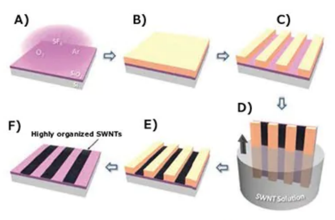
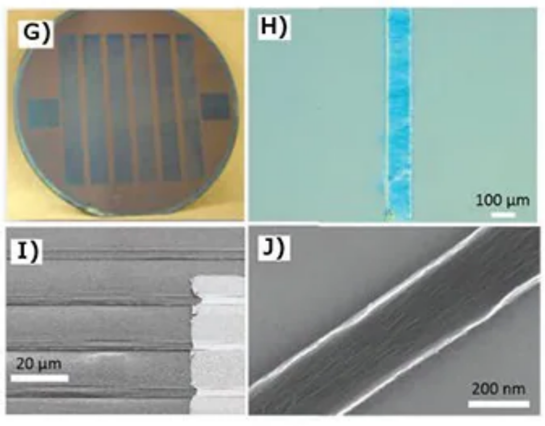
Figure 1: Schematic of template-assisted fluidic SWCNT assembly and SEM images of SWCNT networks. a) surface treatment of SiO2 substrate by plasma etching; B-C) photoresist coating and template patterning; D-E) formation of SWCNT strips by dip coating and assembly of SWCNT strips with photoresist patterns; F) highly organized SWCNT strips after removal of photoresist. G-H) Photographic images of the assembled SWCNT strips on 3 in. wafer and microscopic images of 100 μm wide assembled SWCNT network. I-J) SEM images of 4 μm wide and 200 nm wide assembled SWCNT networks [14,18].
SWCNTS and Si heterojunctions based on optoelectronic applications
The development of Si-based photonic circuit assemblies, such as on-chip sources, modulators, and storage, is a promising approach to address the bottleneck in transmission speed and integration of conventional silicon circuits [19,20]. Here, we show that SWCNT and highly integrated and controlled heterojunctions of silicon can demonstrate a completely unconventional, sharply nonlinear, anti-bias correlated photocurrent. This new phenomenon provides a new way to obtain versatile analog and hybrid digital optoelectronic operations with high switching ratios. Large photocurrent switching can be obtained by small changes in voltage, thus enabling optoelectronic gates/devices with logical outputs depending on the logical state of the optical and electronic inputs. We have demonstrated the photolithographic assembly of many new optoelectronic switches/devices and a large number of SWCNT architecture devices on centimeter-scale wafers. Figures 2A and 2E show schematic and digital photographs of high-density SWCNT/Si heterojunction patterns. SWCNTs are assembled into micro/nanoscale device structures by template-fluidic and conventional lithography on the surface of lightly doped p silicon, as shown in Figure 2F. Figure 2B shows the dark and bright I-V curves of SWCNT-Si junctions, as well as the photocurrent response in metal-Si junctions with similar dimensions. Although the dark I-V in the SWCNT-Si junction follows the conventional diode rectification behavior, the current clearly deviates from the conventional behavior, i.e., it rises sharply by several orders of magnitude within a few volts of the reverse bias voltage Vr, which is different from the luminescent I-V of a conventional metal-Si Schottky junction of the same size at the same light source. The proposed semi-quantitative model of the energy band structure of these heterojunctions suggests that the sharp nonlinear photocurrent behavior may be related to the total number of adjustable n(ε=eVr) of reverse bias in the available states in the SWCNT band. Figure 2C shows a photograph of the SWCNT assembly Si sensor array. Figure 2G shows a forked-finger SWCNT network connected to the source and drain electrodes, which corresponds to two back-to-back photodiodes forming a bidirectional phototransistor. Figure 2H shows a mixed-input photoelectric sum gate, where light and applied voltage are the inputs and the measured current is the output. In addition, Figures 2I-J show a 2- and 4-bit digital optical input, voltage-switchable analog output adder circuit, respectively; when the reverse voltage is applied, the output shows the analog equivalents of the digital sum. Thus, the SWCNT-Si junction is a versatile platform for optoelectronic applications such as photoelectric sensors, optical converters, photometry, and imaging.
Figure 2: Schematic of the new optoelectronic device and images of the SWCNT-Si sensor array. a) SWCNT-Si heterojunction test structure with electrodes (2cm×2cm); b) dark and bright I-V curves of a typical SWCNT-Si heterojunction; c) SWCNT-Si sensor: digital photos of the 0.25 megapixel SWCNT-Si sensor array (array area 12 mm × 12 mm) and D) SEM image of the sensor "core"; E) digital photograph of the SWCNT-Si heterojunction structure; F) SEM image of the assembled SWCNT strip; G) bidirectional phototransistor using a forked-finger SWCNT finger connected to the source-drain lead. The device has an active area of 3 mm × 200 mm; H) with gates for optical and electrical inputs and electrical outputs. The active area of the junction is 3mm x 100mm, illustration: a typical set of operating conditions, determining the "low" and "high" logic states of the input and output conditions; I) a 2-bit adder/or gate with 2 optical inputs and an electrical input and output (J) 4-bit digital-to-analog converters
High performance H2S detector with SWCNT device
SWCNTs have unique nanostructures, high mobility, high current density, and efficient electrochemical surface area, and are the subject of active research for various chemical sensors [8]. Since the original CNT-based chemical sensors utilize only their inherent in order to overcome their limitations in terms of selectivity and sensitivity, functionalization of SWCNT with covalent or non-covalent materials has been used to further improve the sensitivity of SWCNT-based chemical sensors. It is important to note that because of its one-dimensional nanostructure, SWCNT is very sensitive to environmental changes such as humidity and ambient temperature.
In developing the H2S gas sensor, we used TEMPO molecular doping as a catalyst on the surface of SWCNT to improve the sensitivity of H2S detection by redox reaction at room temperature. Figures 3A-D show SEM images of highly organized microsensor devices that were prepared by a template-directed fluidic assembly method followed by a TEMPO coating to pattern a large-scale SWCNT network. Figure 3E shows the chemical structure of the TEMPO used to functionalize the SWCNTs. This compound is capable of oxidizing gaseous H2S and can be used as a sensing molecule for H2S sensors. Figure 3F shows the real-time current variation of the functionalized SWCNT sensor at different concentrations of H2S gas. Figure 3G shows the inherent sensitivity of the device and the advantages of the TEMPO functionalization. Furthermore, according to our results, TEMPO can be oxidized to TEMPO+, a very important product of H2S dissociation. the reduction reaction of TEMPO+ to TEMPO-H is coupled to the dissociation process of H2S to S+2H++2e-, because in air, the SWCNT device exhibits p-type properties due to the oxygen ion (O2). The newly generated electrons are donated to the SWCNT so that it no longer has p-type properties, which makes the functionalized SWCNT more sensitive than the pure SWCNT. In addition, we found that humidity improves the sensitivity of H2S by improving the change from TEMPO to TEMPO+. Finally, this paper also demonstrates the high responsiveness of SWCNT devices functionalized with TEMPO to H2S gas with increasing humidity. This is particularly true for semi-single-walled carbon nanotubes, which exhibit a high sensitivity of up to 420% at 60% humidity.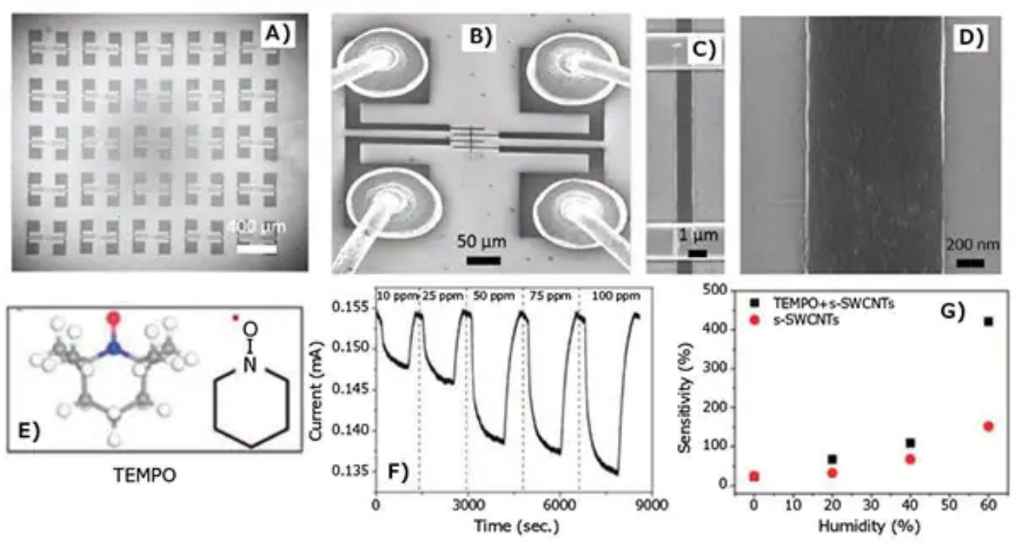
Figure 3: High performance H2S detector based on SWCNT network. a-d) SEM images of the assembled SWCNT device array; e) chemical structure of the TEMPO molecule; f) variation of the real-time current of the functionalized SWCNT sensor with H2S gas concentration; g) sensitivity of the unmodified SWCNT device and the TEMPO functionalized SWCNT device with humidity of the SWCNT devices [16].
Electrofusion of SWCNT networks: inter-isomeric transformations
The modification of sp2 structured carbon nanotubes usually requires extreme and difficult to control conditions such as high temperature, high pressure and high energy irradiation. In this paper, we propose a simple but powerful electrical method to structurally transform carbon nanotubes from SWCNT to multi-walled carbon nanotubes (MWCNT) or multilayer graphene/graphite nanoribbon structures (MGNR) by applying controlled AC voltage pulses.
By controlling the size of the voltage pulse, the source time and the number of switching cycles applied to the SWCNT network, the target transformed nanostructures (MWCNTs or GNRs) can be obtained without creating any structural defects. It was also found that the electrical conductivity (up to 35% resistance drop) and thermal conductivity (up to 6-7 times the thermal conductivity, 300 W/mK) of the SWCNT network were greatly improved after structural modification. Figure 4A shows the structure of the SWCNT network assembled with metal electrodes on a TEM grid. Figure 4B shows the I-V curves, maximum current density and breakdown voltage (Vb) of the SWCNT network. Figure 4C shows the time-dependent AC voltage pulses applied to the SWCNT device. Figures 4D-F show TEM images of the original SWCNT, MWNT (0.6Vb, 3,000 cycles) and GNR (0.8Vb, 3,000 cycles) after the electrofusion process. Figure 4G-H shows the resistance change and thermal conductivity of SWCNT devices at different applied voltages for the same 3,000 cycles.
Figure 4: Pulsed alternating voltage induced isomeric transformation of SWCNT and its electrical and thermal properties A) SEM image of the assembled SWCNT network with electrodes integrated on a specially designed TEM grid; B) typical I-V characteristics of the original SWCNT network device showing the electrical breakdown behavior, where Vb is the breakdown voltage; C) time-varying AC voltage pulses for structural transformation of SWCNT networks; D) TEM images of pristine SWCNT; E) TEM images of multi-walled structures after 3,000 cycles with applied voltage Va = 0.6Vb; F) TEM images of multilayer graphite nanoribbons after 3,000 cycles with Va = 0.8Vb; G-H) electrical and thermal properties [17].
CONCLUSIONS
In this paper, the authors proposed a highly organized SWCNT network for template-guided fluidic assembly. Using lithography-patterned template-assisted dip-coating, SWCNTs are assembled directly between pre-designed micro- and nanoscale photoresist channels using a lithography-patterned template-assisted dip-coating method to form densely arranged side networks of SWCNTs with different geometries with feature sizes ranging from 150 nm to hundreds of micrometer scales. These highly organized micro- and nanoscale SWCNT network structures can be integrated into a variety of sensor device architectures. The room temperature and wafer-level scaling compatibility of the stencil-guided fluidic assembly technique offers the possibility of reproducibility on a large scale. In this context, this paper demonstrates a high-performance photodetector and a novel logic device based on SWCNT and a scalable heterojunction in silicon, whose output current can be fully controlled by optical and electrical inputs. We also present a SWCNT-based chemical sensor that can effectively detect H2S gas through a redox reaction occurring on a SWCNT network functionalized using TEMPO as a catalyst.
Finally, the authors demonstrate precisely controlled and well-defined isotropic transitions and molecular junction formation on a large-area SWCNT network using controlled AC voltage pulses. Using this newly developed electrical process, small-diameter SWCNT can be selectively transformed into other isotropic sp2 nanostructures, such as multi-walled carbon nanotubes, multilayer graphene nanoribbons, and structures with sp3 bonds.
References
1.Iijima S. 1991. Helical microtubules of graphitic carbon. Nature. 354(6348):56-58. http://dx.doi.org/10.1038/354056a0
2.Avouris P. 2002. Molecular Electronics with Carbon Nanotubes. Acc. Chem. Res. 35(12):1026-1034. http://dx.doi.org/10.1021/ar010152e
3.Dai H. 2002. Carbon Nanotubes: Synthesis, Integration, and Properties. Acc. Chem. Res. 35(12):1035-1044. http://dx.doi.org/10.1021/ar0101640
4.Yao Z, Kane CL, Dekker C. High-Field Electrical Transport in Single-Wall Carbon Nanotubes. Phys. Rev. Lett. 84(13):2941-2944. http://dx.doi.org/10.1103/physrevlett.84.2941
5.White CT, Todorov TN. 1998. Carbon nanotubes as long ballistic conductors. Nature. 393(6682):240-242. http://dx.doi.org/10.1038/30420
6.Pop E, Mann D, Wang Q, Goodson K, Dai H. 2006. Thermal Conductance of an Individual Single-Wall Carbon Nanotube above Room Temperature. Nano Lett. 6(1):96-100. http://dx.doi.org/10.1021/nl052145f
7.Lu JP. 1997. Elastic properties of single and multilayered nanotubes. Journal of Physics and Chemistry of Solids. 58(11):1649-1652. http://dx.doi.org/10.1016/s0022-3697(97)00045-0
8.Kong J. 2000. Nanotube Molecular Wires as Chemical Sensors. 287(5453):622-625. http://dx.doi.org/10.1126/science.287.5453.622
9.Wen L, Li F, Cheng H. 2016. Carbon Nanotubes and Graphene for Flexible Electrochemical Energy Storage: from Materials to Devices. Adv.Mater. 28(22):4306-4337. http://dx.doi.org/10.1002/adma.201504225
10.Fan S. 1999. Self-Oriented Regular Arrays of Carbon Nanotubes and Their Field Emission Properties. 283(5401):512-514. http://dx.doi.org/10.1126/science.283.5401.512
11.Shi Kam NW, O'Connell M, Wisdom JA, Dai H. 2005. Carbon nanotubes as multifunctional biological transporters and near-infrared agents for selective cancer cell destruction. Proceedings of the National Academy of Sciences. 102(33):11600-11605. http://dx.doi.org/10.1073/pnas.0502680102
12.Jaber-Ansari L, Hahm MG, Somu S, Sanz YE, Busnaina A, Jung YJ. 2009. Mechanism of Very Large-Scale Assembly of SWNTs in Template Guided Fluidic Assembly Process. J. Am. Chem. Soc. 131(2):804-808. http://dx.doi.org/10.1021/ja8076523
13.Xiong X, Chen C, Ryan P, Busnaina AA, Jung YJ, Dokmeci MR. 2009. Directed assembly of high density single-walled carbon nanotube patterns on flexible polymer substrates. Nanotechnology. 20(29):295302. http://dx.doi.org/10.1088/0957-4484/20/29/295302
14.Jaber-Ansari L, Hahm MG, Kim TH, Somu S, Busnaina A, Jung YJ. 2009. Large scale highly organized single-walled carbon nanotube networks for electrical devices. Appl. Phys. A. 96(2):373-377. http://dx.doi.org/10.1007/s00339-009-5194-2
15.Kim YL, Jung HY, Park S, Li B, Liu F, Hao J, Kwon Y, Jung YJ, Kar S. 2014. Voltage-switchable photocurrents in single-walled carbon nanotube? silicon junctions for analog and digital optoelectronics. Nature Photon. 8(3):239-243. http://dx.doi.org/10.1038/nphoton.2014.1
16.Jung HY, Kim YL, Park S, Datar A, Lee H, Huang J, Somu S, Busnaina A, Jung YJ, Kwon Y. 2013. High-performance H2S detection by redox reactions in semiconducting carbon nanotube-based devices. Analyst. 138(23):7206. http://dx.doi.org/10.1039/c3an01762a
17.Jung HY, Araujo PT, Kim YL, Jung SM, Jia X, Hong S, Ahn CW, Kong J, Dresselhaus MS, Kar S, et al. 2014. Sculpting carbon bonds for allotropic transformation through solid-state re-engineering of sp2 carbon. Nat Commun. 5(1): http://dx.doi.org/10.1038/ncomms5941
18.Kim YL, Li B, An X, Hahm MG, Chen L, Washington M, Ajayan PM, Nayak SK, Busnaina A, Kar S, et al. 2009. Highly Aligned Scalable Platinum-Decorated Single-Wall Carbon Nanotube Arrays for Nanoscale Electrical Interconnects. ACS Nano. 3(9):2818-2826. http://dx.doi.org/10.1021/nn9007753
19.Almeida VR, Barrios CA, Panepucci RR, Lipson M. 2004. All-optical control of light on a silicon chip. Nature. 431(7012):1081-1084. http://dx.doi.org/10.1038/nature02921
20.Liu L, Kumar R, Huybrechts K, Spuesens T, Roelkens G, Geluk E, de Vries T, Regreny P, Van Thourhout D, Baets R, et al. 2010. An ultra-small, low-power, all-optical flip-flop memory on a silicon chip. Nature Photon. 4(3):182-187. http://dx.doi.org/10.1038/nphoton.2009.268