Creating an account has many benefits:
- See order and shipping status
- Track order history
- Check out faster
Popular Semiconductor Materials: Application Introduction of Gallium Arsenide

Background
Gallium arsenide (GaAs) (Item No.:G119227) is a compound made of two elements, gallium and arsenic, which are important group IIIA and VA semiconductor materials. Therefore, GaAs is also an important compound semiconductor material, GaAs has a bright gray appearance, metallic luster, brittle and hard. It is stable at room temperature and does not react with hydrochloric acid, sulfuric acid and hydrofluoric acid, but can react with concentrated nitric acid and also with hot hydrochloric acid(Item No.:H399545) and sulfuric acid(Item No.:S399850). When it is heated to 873K, the appearance begins to generate oxides and form oxide films. In addition, GaAs also has better electronic properties, such as higher saturation electron rate and electron mobility, faster switching speed, resistance to natural radiation and a series of unique properties.
GaAs is naturally scarce and is usually obtained by direct gallium and arsenic synthesis, of which horizontal zone melting is a common method. Single crystals can be obtained by regional purification. GaAs can also be obtained by indirect methods, such as GaCl(Item No.:G345285) reduction by arsenic vapor(Item No.:A110123) (Eq. 1), or GaAs by thermal decomposition of Ga(CH3) and AsH3 at a certain temperature (Eq. 2).
4GaCl + 2H2 + As4 → 4GaAs + 4HCl (i)
Ga (CH3)3 + AsH3 → GaAs + 3CH4 (ii)
Applications
GaAs has many excellent characteristics and its applications are very broad, which can be broadly divided into four major areas: RF (radio frequency), PHOTONICS (optoelectronics), LED (light emitting diode) and PV (photovoltaic power generation).
RF Devices
The main function of RF devices is to achieve signal transmission and reception, by the power amplifier (Power Amplifier, PA), RF switches, filters, digital-to-analog/analog- to-digital converters and other devices. GaAs is used in the field of RF, the main link is the PA. after the PA amplified signal, and finally emitted from the device, belongs to the communication equipment high energy link.
Recently, Nguyen et al. [1] designed a stacked field-effect transistor PA with a harmonic tuned output matching network using 0.15 μm GaAs. the prepared PA has 28.5 dBm output power, 12 dB gain, and 38.4% power-added efficiency (PAE). This is the first time that stacked field-effect transistor technology is combined with a harmonic tuned output network to achieve high PAE and highly power density in a GaAs PA.
Figure 1: Power amplifier chip photo (1.1 mm × 0.8 mm)[1]
In addition, GaAs also occupies a dominant position in the field of 5G cell
phone PA. GaAs has higher saturation electron rate and electron mobility, which
makes it suitable for application in high frequency scenarios and has lower
noise in high frequency operation; at the same time, because GaAs has higher
breakdown voltage than Si, so GaAs is more suitable for application in high
power situations. Because of these characteristics, GaAs in the 5G era, will
still be the main material for power amplifiers and RF switches and other cell
phone RF devices.
Optical Devices
Another advantage of GaAs is its direct energy gap, which gives it a better
optoelectronic performance and can be used to make optoelectronic devices.
Infrared lasers and sensors made using GaAs substrates have received a lot of
attention because of their highly power density, low energy consumption, high
temperature resistance, high luminescence efficiency, high breakdown voltage
and other characteristics.
Efficient photovoltaic conversion is a relentlessly pursued goal, and is of great importance in promoting the development and application of new energy and information fields. Photonic power converters or photoelectric sensors can absorb the infrared laser power transmitted through a multimode fiber and convert it to electrical power for remote use. To convert this power into a useful voltage, Hinzer et al. [2] designed and fabricated a GaAs photovoltaic photovoltaic sensor that uses a single, lattice-matched, vertically stacked single-cell device to generate >5 V, thereby eliminating complex fabrication and assembly steps. Experimental measurements also show conversion efficiencies of up to 60.1% at a wavelength of 835 nm and a light intensity of 11 W/cm2.
Figure 2: Schematic diagram of the experimental setup [2]
LED devices
Light-emitting diode (LED) is a solid light-emitting device composed of compound semiconductors (GaAs, GaN, etc.), which can convert electrical energy into light energy. LEDs made of different materials emit different wavelengths and colors of light. LEDs can be distinguished into conventional LEDs, Mini LEDs, Micro LEDs and other types according to chip size, among which Mini LEDs and Micro LEDs are used in the new generation of displays.
Electroluminescence (electron to photon conversion in LEDs) can be used as a refrigeration mechanism provided that the LEDs have a high quantum efficiency. Xiao et al. [3] investigated the practical application of electroluminescence in refrigeration by optimizing GaAs/GaInP double hetero-structured LEDs. The study firstly developed a design model based on fine equilibrium physics and statistical ray optics methods, and predicted an external luminescence efficiency 97.7% at 263 K. Second, to improve the performance of the cooling factor, the researchers further paired cooled LED with a photovoltaic cell that converts part of the emitted light energy into electrical energy. For applications near room temperature and moderate power density (1.0-10mW/cm2), the electroluminescent cooler can operate with a higher performance factor (predicted to be 1.7 times higher) using the material mass in the existing GaAs device.
GaAs is a III-V compound semiconductor material with a suitable energy gap to match the solar spectrum and can withstand high temperatures. Compared with silicon solar cells, GaAs solar cells have better performance.
As shown in Figure 4, Sheng and colleagues [4] prepared a miniature thin-film double junction GaAs photodiode device and investigated its photon and carrier transport behavior under different wavelengths and intensities of excitation light. The experimental tests show that the photon recycling effect is closely related to the excitation light wavelength and power, and the photocurrent and excitation light power of the double-junction cell show super linear and linear characteristics under blue-violet light (400-480 nm) and near-infrared light (~800 nm) irradiation, respectively. Meanwhile, the photon recycling effect can significantly improve the current matching between sub-cells under high-intensity excitation light irradiation to achieve a broad-band, high-efficiency photovoltaic response (wavelength 400~800 nm, external quantum efficiency close to 50%).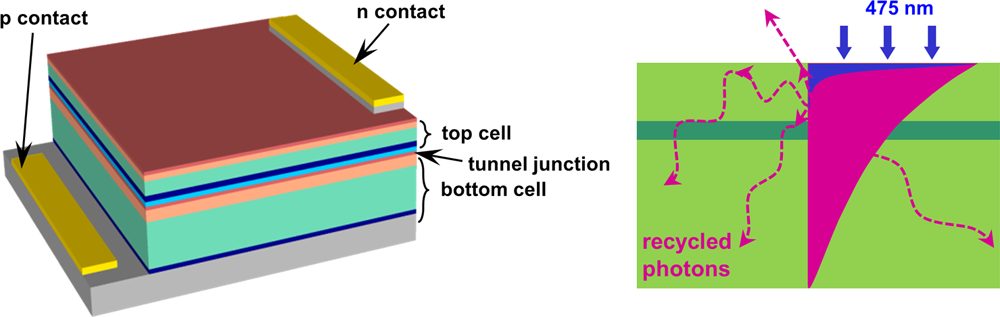
Figure 4: Schematic diagram of the optical process inside a GaAs double-junction photodiode under 475 nm illumination [4]
Figure 5: Schematic diagram of PV/T heterojunction: (a) Separate channel system;
(b) Dual channel system[5]
In terms of commercial applications, due to the high manufacturing cost of GaAs, terrestrial PV plants are rarely used. However, the current new growth technology has greatly shortened the time to make solar cells, which is expected to bring down the process cost significantly and make the large-scale commercial use of GaAs cells possible.
References
2. Valdivia C E, Wilkins M M, Bouzazi B, et al. Five-volt vertically-stacked, single-cell GaAs photonic power converter[C]//Physics, Simulation, and Photonic Engineering of Photovoltaic Devices IV. SPIE, 2015, 9358: 48-55. https://doi.org/10.1117/12.2079824
3. Xiao T P, Chen K, Santhanam P, et al. Electroluminescent refrigeration by ultra-efficient GaAs light-emitting diodes[J]. Journal of Applied Physics, 2018, 123(17): 173104. https://doi.org/10.1063/1.5019764
4. Ding H, Hong H, Cheng D, et al. Power-and spectral-dependent photon-recycling effects in a double-junction gallium arsenide photodiode[J]. ACS Photonics, 2019, 6(1): 59-65. https://doi.org/10.1021/acsphotonics.8b01404
5. Hassani S, Taylor R A, Mekhilef S, et al. A cascade nanofluid-based PV/T system with optimized optical and thermal properties[J]. Energy, 2016, 112: 963-975. https://doi.org/10.1016/j.energy.2016.06.142
Aladdin:https://www.aladdinsci.com
- Help & Customer Service
- FAQs
- What do the terms MSDS, SDS, COA, and TDS in the chemical industry mean? How do they differ?
- What is the purpose of an isotype control? How are they selected?
- Why are our chemicals so much less expensive than the same chemicals sold by your competitors?
- What are MSDS and SDS?
- What are the requirements to become an Aladdin distributor?
- Are there any discounts or sales rebates for distributors?
- What is the duration of the distributor agreement?
- Will I receive training and support as a distributor?
- Under which law is the distributor agreement governed?
- The differences between registered users(with a profile) and non registered users
- Delivery and receipt specification
- What is a third -party express or logistics company delivery?
- My order was charged the freight. If the return in the later period, will the previous freight be refunded to me?
- What should I do if the goods are less/the product is wrong?
- What should these products be used for and who should use them?
- Why are chlorophosphonate liposomes useful for studying macrophage function?
- What is the CAS number?
- What dose of antagonist, agonist, or signaling tool should be used in vivo?
- Aladdin product purity and quality: what is it and how is it determined?
- What dose of an antagonist, agonist, or signaling tool should be used in vitro?
- How do I determine if a compound is cell-permeable?
- What should I do if I can't see any product in the vial?
- Should different batches of a product look the same?
- What is the molecular weight and molecular formula?
- How do I dissolve my product?
- How should I store my product?
- Effects of storage on solubility
- Why does Aladdin‘s Biochemicals sometimes ship chemicals at room temperature when the vial is labelled 'store at +4°C or -20°C'?
- What is the half-life of clodronate (liposomes)?
- Pack sizes and weighing accuracy: do I need to reweigh my product?
- I did not observe macrophage depletion, what can be the reason?
- My animal has died immediately after injection of (clodronate) liposomes。
- How to know how much peptide is in my vial?
- My animal has died several hours or days after injection of (clodronate) liposomes.
- How should I store and use lyophilized peptides?
- How should l store the liposomal suspension?
- What is the concentration of the clodronate liposome suspension?
- How should I dissolve and store peptide solution?
- What is the size and charge of the liposomes?
- ln which medium are the liposomes suspended?
- Dissolved amino acids: how to prepare a solution with 1 equivalent of NaOH?
- How can l detect the Dil-labeled liposomes?
- What types of experiments are our products eligible for?
- I need the SDS and Certificate of Analysis for the product that I purchased.
- Where can I get protocols for using your products?
- GHS Classification
- How to obtain a quality inspection certificate (COA)?
- Does aladdin test for endotoxin in their antibodies?
- What should I know about the stability of your protein products?
- Which isotype are Aladdin’s polyclonal antibodies?
- What endotoxin level should be expected when purchasing Aladdin proteins?
- How are your antibodies purified?
- Why can’t I see the protein pellet in the vial?
- Can you tell me what epitope your antibody binds to?
- Which cytokines show cross-species activity?
- Have Aladdin’s antibodies been tested in neutralization assays?
- What is the relationship between the specific activity expressed as an ED50 and as units/mg?
- Are Aladdin’s antibodies suitable for use in ELISA and Western Blot applications?
- What information should be known about the stability of your antibody products?
- Do Aladdin’s antibody products contain any carrier proteins or other additives?
- What is the relationship between specific activity units and International Units of activity?
- How does Aladdin obtain International Units of activity?
- Will Aladdin antibodies work in immunohistochemistry and immunocytochemistry applications?
- Will Aladdin antibodies recognize target proteins sold by other vendors?
- Will Aladdin antibodies recognize target protein in complex biological fluids such as blood or serum?
- What are the differences between encapsulation efficiency, loading capacity, and yield?
- How can micelle stability be improved?
- Can nanoparticles be used for oral drug delivery?
- What is the ideal size for a nanocarrier?
- What strategies can be used for the extended release of peptides for one month or more?
- When considering PEGylation for a protein drug, how do you decide what PEGylation chemistry to use?
- What are Building Blocks?
- What are the applications of Building Blocks in drug development?
- What are the common types of drug Building Blocks?
- What are the substituted functional groups of the Building Blocks?
- What role do Building Blocks play in new drug development?
- Which Building Blocks are more popular in medicinal chemistry?
- What are the main competition barriers of molecular Building Blocks industry?
- What is the application scale of molecular Building Blocks in drug development?
- What are the targets of molecular Building Blocks?
- What are the synthetic techniques of molecular Building Blocks?
- My DMSO-d6 appears to be a solid. What can I do?
- How can I measure acidity levels in D2O solutions?
- Should my NMR solvents be handled in a special way?
- Does my isotope solvent require special storage?
- What are the 3 most commonly purchased isotopes in trace element analysis and their quantity of supply?
- What type of mineral oil is contained in the 6Li metal, and how would this be removed?
- What are the key criteria for selecting stable isotope-labeled standards for clinical measurements?
- What is meant by descriptions such as TC treated/no TC treated that appear in product descriptions such as cell culture dishes?
- Which surface should I use to grow suspension cells?
- How should closed-cap cell culture flasks be used? What is the difference between the use of the lid with the filter membrane?
- What do we often hear about T25 or T175?
- I used i-Quip® surface treated culture bottle/dish/plate, the cells do not adhere to the surface, is it a product quality problem?
- After removal from the liquid nitrogen tank, the cell cryogenic vials will occasionally burst. How to avoid it?
- What precautions should be taken when using cell cryogenic vials?
- What are the possible reasons for the cracking phenomenon of the centrifuge tube during centrifugation?
- Why is it necessary to add carrier protein to some recombinant protein solutions?
- Will glycosylation affect the biological activity of recombinant protein?
- How to operate the reconstitution and preservation of recombinant protein?
- How can I save the recombinant protein after re-dissolution?
- What are the main differences between the recombinant proteins produced by different expression systems?
- Why didn't I detect the activity of the recombinant protein in the experiment?
- Can recombinant proteins of different species be cross-used?
- What is the role of the protein tag? Does the fusion tag need to be removed during the experiment?
- Is it possible to use the vortex shaker to help the lyophilized powder fully dissolve?
- What is Friedel Craft reaction with example?
- What are the advantages of Friedel Crafts acylation?
- Is Friedel-Crafts alkylation reversible?
- How is a Lewis acid used in Friedel Crafts acylation?
- What is alkylation of benzene?
- Why does nitrobenzene not undergo the Friedel-Crafts acylation reaction?
- What are the limitations of Foucault alkylation reaction?
- What are the limitations of the Foucault acylation reaction?
- What is COA?
- Distinguishing between MSDS, COA, and TDS?
- How can I get a trial size product for free?
- Is there a limit to how many free trial size products I can receive?
- Will I have to pay anything for the trial size product?
- How will I receive the discount coupon?
- Can the discount coupon be used for any product?
- How do I apply to become an Aladdin distributor?
- What is the process after submitting the distributor application?
- Can I return products? What is the return policy?
- What happens if either party wants to terminate the agreement?
- Is there a confidentiality clause in the distributor agreement?
- Does the flow-through antibody to CD206 need to be fixed to break the membrane?
- Are CD8 and CD8α the same indicator?
- Is CD4(domain 1) CD4?
- Is CD44H a CD44?
- Is CD3ε a CD3?
- Is CD45.1/ CD45.2 a CD45?
- What is the difference between Mouse CD90 and CD90.1 and CD90.2?
- What is the difference between Human CD45RA and CD45RO?
- What is the concentration of the primary antibody?
- What does IHC mean on the data sheet? Is it frozen section? Is it different from IHC-F?
- How many slices can I do with 20μI when I have IHC lab-applicable antibodies?
- If the species of my experimental sample is not included in the Reactivity of the antibody, is there any after-sales service available?
- Can the antibody be used in applications that are not described in the package insert?
- How should I choose the secondary antibody?
- How to choose positive controls for antibodies?
- There is a disagreement between the molecular weight of the literature check and the specification, why are there several molecular weights for the same indicator?
- IHC experiment, wondering what are the antigen repair conditions? Should I use EDTA or potassium citrate?
- Can the protein be shipped as a lyophilized powder?Can it be shipped as liquid?
- What are the transportation conditions for proteins?
- Can proteins be used in cell culture/injected mice?
- Does the protein Buffer contain denaturants?
- Are recombinant proteins active? Is it possible to do an activity test?
- By what way are proteins purified?
- Label-free protein purification method?
- What concentration of BSA is recommended for WB experiments?
- How long does the BSA stay closed at room temperature?
- Lysate would like to ask what PMSF does with Na3VO4?
- Lysate lysate not lysed, add ripa and shake, then lysed on ice for 20 minutes and then centrifuged and got a gooey mess?
- How many cells are lysed in 100μl of RIPA protein lysate?
- Can cell lysate lysed cells be followed by immunoprecipitation?
- Can the lysate be used without sodium aluminate?
- Can I keep the protein at -20°C for a month after cooking with loding buffer?
- Can ECL be used in ELISA?
- How long can I keep it at -20°C? Can it be stored for a short time at 4°C or room temperature? Can it be stored at -80°C?
- Can I still use it if I accidentally store it at room temperature for a day?
- If I accidentally boil the 5x Sampling Buffer for 15min, is it still usable?
- Does the sample buffer have an effect on the effectiveness of the electrophoresis solution? If the buffer is accidentally run out does it need to replace the electrophoresis solution?
- Is it feasible to boil and denature proteins before adding protein upload buffer?
- Sediment has been found in this product, can I continue to use it? What should be done?
- Does the protein's own charge affect the buffer?
- If the concentration of the denatured sample is high, how should it be diluted?
- If the protein contains polymer heterobands, dimers may be present, do I need to add doubling buffer to open the dimers?
- When electrophoresis is performed on a sample denatured with buffer, if the sample does not move when the sample volume is high, and if the sample volume is low, the sample runs fast and unevenly, how to solve the problem?
- What is the reason that the protein added to the buffer cooks without precipitation, but the next day when the sample is removed and spiked, precipitation appears? What should be done?
- After lysing the cells first with the lysate, add 5x upsampling buffer in a 4:1 volume, then water bath denaturation is it better to use a 100 degree water bath or a 95 degree water bath?
- After adding buffer to boil denatured proteins for cryopreservation, do they still need to be boiled after they are removed again? Why?
- How can I quickly remove the bromophenol blue that may be obscuring the bands at the end of the gel run?
- What is the reason why the protein after denaturation by adding buffer tends to be difficult to sink and float up easily when spotting? What should I do to solve this problem?
- When extracting proteins from suspension cells, can I add the product directly to boil and denature them?
- Can it be used in non-denaturing electrophoresis?
- Is there a requirement for protein concentration for this product? If the protein concentration is high, do I need to increase the concentration of the buffer?
- After the protein sample has been spiked with Sampling Buffer, boiled at 95°C for 10 min, and centrifuged at 14,000, individual samples will be delaminated prior to sampling, what is the reason for this?
- Protein samples boiled in buffer are blue in color and turn blue-violet after being left at -80°C. What is the reason for this? Does it affect the subsequent electrophoresis?
- BCA concentration measured protein concentration 3mg/ml, but after adding buffer found no protein bands appeared, what is the reason?
- Do I need to add extra mercaptoethanol before using this product?
- At what temperature is the pH 7 .4 of RIPA lysis buffer measured?
- Does RIPA lysis buffer contain reducing agents such as DTT or mercaptoethanol?
- Can RIPA lysis buffer continue to be used after being stored unopened at room temperature for 24 hours? Is there a limit to the number of repeated freezing and thawing?
- Is this lysate suitable for extracting mitochondrial proteins?
- What are the temperature requirements for eluting antibodies in an antibody removal solution? Can the same membrane be eluted more than once?
- Can DAPI be excited with laser confocal λ=405nm after staining the nucleus?
- Can this product be used directly for staining of adherent cells? Can it be used to stain live cells and determine apoptosis by staining?
- Do I need to adjust the pH again after diluting EDTA Antigen Repair Solution?
- Will the pH value change after diluting the product into a working solution?
- What solution should be used to dissolve Proteinase K when used? What is the common working concentration? At what degree does it need to be stored?
- Does Proteinase K powder need to be protected from light when storing and weighing?
- Can tumor tissue cuts be stored for a long time after fixation in 4% paraformaldehyde fixative at room temperature?
- Does paraformaldehyde fixation disrupt cell membranes?
- What is the difference between CD62L and CD62?
- After fixing the cells at room temperature for 15 min with this 4% paraformaldehyde, the cell membrane blisters, do I need to change the fixation temperature to 4°C?
- What do I need to be aware of when storing paraformaldehyde? Is it volatile?
- What is the difference between E-AB-F1272D PE Anti-Mouse lL-17AAntibody[17F3] and EAB-F1199D PE Anti-Mouse lL-17AAntibody[TC11-18H10.1] are different?
- How much Tween needs to be added if I want to use this TBS to prepare TBST?
- What are the recommendations for flow assay of mouse macrophages to detect M1 and M2 types of macrophages?
- Is there a requirement for the mouse strain for the cell flow antibody, since we are experimenting with C57BL6N mice, is it special?
- Does this Hematoxylin Staining Solution need to be diluted for use?
- What related reagents are needed for flow-through staining?
- What should I do if I find that this dye solution produces precipitation? How can I tell if the dye has failed?
- What kind of samples need sealer? Should I wash them after sealing?
- What concentration of Triton X-100 is typically needed for cell lysis? What solutions are typically used for dilution?
- Does WB Primary Antibody Diluent contain sodium azide?
- Is the gel stained with this stain compatible with in-gel digestion and mass spectrometry?
- What is the reason that the blue color is hard to come off after half an hour of dyeing glue with this dye solution? How to solve it?
- How does the sealer work?
- How many times can this stain be reused?
- How is the cell staining buffer used and can I use PBS instead? How much cell staining buffer do I need for one sample?
- How should the experimental groupings/controls be set up?
- How do I dilute the Test-packed antibodies?
- What is the difference between our Flow Antibodies available in Test packages and μg packages?
- The Illuminating the Druggable Genome (IDG)
- The amount of cells is not 1x10^6, only 1x10^5, can the amount of antibody be reduced?
- Can flow antibodies be used when stored at -20°C and then thawed?
- Why centrifuge before use?
- What do host species and species reactivity mean, respectively?
- What are the requirements of sample preparation for the use of centrifuges?
- What is the best way to choose between the different clone numbers of CD4?
- What are the markers for sorting Raw264.7 M1 and M2 cells by flow cytometry? Can they be cultured after sorting?
- I want to test for tumor-associated macrophages, is it okay to use only the F4/80 test?
- If I need to label an antibody with SMCC-activated R-phycoerythrinand then use the antibody coupled with phycoerythrin as an ELISA, what other reagents are needed? Is there a specific procedure?
- Can Erythrocyte Lysate be used on avian erythrocytes?
- Can Erythrocyte Lysate be used at room temperature?
- I want to stain CD206 and need to break the membrane, so should I use cytokine fixative or transcription factor fixative?
- Which is a better sealer, mouse sealer CD16/32 or unmodified mouse whole lgG antibody?
- Is it okay to dilute the rupture agent in intracellular fixation rupture agent with cell staining buffer?
- I want to obtain rare cells other than red blood cells and white blood cells in my sample and keep the original cell viability of the rare cells, is this lysate suitable?
- Isoform controls help eliminate nonspecific staining, so how do you set the door?
- Do I need an isotype control for all treatment groups, e.g.: 12h group, 24h group?
- How do I set up an FMO combined isotype control?
- Is the mouse Fc blocker in μg packaging and is it powdery in nature? Does it dissolve in pbs?
- I purchased three flow-through antibodies, all sized at 50 μg, how many samples can I make?
- Do I need to do a live and dead dye on my sample to eliminate dead cells? What will happen if I don't?
- The client's cells themselves are not fluorescent, but the drug being processed is fluorescent, how does the client go about determining what the drug is fluorescent?
- I want to do a spleen flow-through, and I can't flow-through on the machine until tomorrow after picking up the sample today, how should I store the sample?
- I only have 2.5×10^5 cells in my cell sample, do I only need to use 1.25 μL of flow-through antibody?
- How should I remove platelets from my blood? Can red blood cell lysate be used?
- Is calcium ion-containing HBSS an option for the preparation of mouse tumor single cell suspensions?
- What are the precautions for human peripheral blood testing for intracellular factor?
- What are the considerations for testing tissue samples for intracellular indicators?
- There are two orders of cleavage red for sample preparation, cleavage red followed by staining and staining followed by cleavage red, what to choose?
- My samples are peripheral blood and alveolar lavage fluid from mice, how can I preserve the samples for the maximum amount of time after I remove them?
- When do you use sterile supplies for flow-through antibody samples?
- How to Cite Aladdin Scientific Products and Website in Your Published Work?
- I Would like a compatibility table tailored to specific instruments and their configurations for Fluo™ dyes?
- Product Origin Information & FAQ for Aladdin Scientific
- What's different between CHEMBL13035 and SCHEMBL122822, why does SCHEMBL122822 has an extra "S" at the beginning?
- What if I encounter issues using my discount coupon?
- What types of targets are there?
- read more
- Technical articles
- Targeted protein degradation technology: proprietary drugs are not difficult, drug resistance is no longer
- Strain-promoted alkyne-nitrone cycloaddition (SPANC)
- A bridge to protein science——Aladdin@Polypeptide
- Fluorescent probes – brightening the horizon of biomedical research
- Method and Precautions of SDS-PAGE Gel Preparation
- Aladdin® Plant Research Related Products
- DEAE-Dextran
- IgG
- Dextran Chemistry
- liposomes
- Hyaluronan
- Macrophage Stimulating Protein (MSP)
- Click Chemistry
- BINOL and Derivatives
- Linkers - A Crucial Factor in Antibody–Drug Conjugates
- Karl Fischer Titration to Measure the Water Content of Samples that Do not Readily Release Water
- Application of Gold Catalysts in Industrial Hydrogenation Process
- N-Heterocyclic Carbene (NHC) Ligands
- Applications of Nanoparticles in Pathogen Detection and Identification
- Cannizzaro Reaction
- Clemmensen Reduction
- Guide to Adherent Cell Culture Basics: Seeding, Expanding, and Harvesting
- Application of Granular Materials in Immunoassay
- Properties and Applications of Magnetic Nanoparticle
- Wolff-Kishner Reduction
- Fries rearrangement
- Sulfonyl Chlorides and Sulfonamides
- Alzheimer’s Disease Signaling
- DNA Damage and Repair
- How To Improve the Safety of Electrolyte in Lithium-Ion Batteries?
- Research Progress of High-Voltage Lithium-Ion Battery Materials
- Application of Magnetic Nanoparticles in Protein Expression
- Silica-Coated Gold Nanoparticles: Surface Chemistry, Properties, Benefits, and Applications
- Application of albumin
- Friedel–Crafts Acylation
- Immunoprecipitation technology
- Aldol Condensation Reaction
- Basic Concepts about Catalysts
- Baeyer-Villiger Oxidation
- Cinchona Alkaloids
- Application of Magnetic Particles in Organelle Separation
- Nicewicz Photoredox Catalysts for Anti-Markovnikov Alkene Hydrofunctionalization
- Application of Magnetic Nanoparticles in RNA and DNA Separation
- Homobenzotetramisole (HBTM): A General Organocatalyst for Asymmetric Acylations
- Nanoparticle-Based Small Molecule Drug Delivery
- Visible Light Photoredox Catalysts
- Applications of Nanoparticles in Vaccine Delivery
- Markovnikov’s Rule
- Grignard Reagent
- Neurotransmitters, Receptors, and Transporters
- Hydrogenation Catalysts
- Organic Photoredox Catalysts for Visible Light-Driven Polymer and Small Molecule Synthesis
- Knoevenagel Condensation Reaction
- Grignard reaction
- Nanoparticle-Based Gene Delivery
- Regulation of TGF-beta activity by BMP-1
- Retinoic Acid and Gene Expression
- Guide to Sialylation: I Neu5Ac and Neu5Gc Quantitation
- Guide to Sialylation: II Highly Sialylated Glycoproteins
- Quantitative Sialic Acid Analysis
- SuFEx: Sulfonyl Fluorides that Participate in the Next Click Reaction
- Reductive Amination with 2-picoline-borane Complex
- Copper-Free Click Chemistry
- Mesoporous Materials: Properties and Applications
- Media and Supplements in Cell Culture
- Quantum dots
- Materials for Advanced Thermoelectrics
- Application of Graphene in Photocatalysis
- Silver Nanomaterials for Biological Applications
- Stripping and Reprobing Western Blotting Membranes
- Graphene Inks for Printed Electronics
- Procainamide Labeling Kit-2-Picoline Borane-24T
- Procainamide Labeling Kit-Sodium Cyanoborohydride-24T
- Procainamide Labeling Kit-Sodium cyanoborohydride-96T
- Permethylation Kit
- 2-AB Labeling Kits-Sodium Cyanoborohydride
- 2-AB Labeling Kits-2-Picoline Borane
- Buffer Reference Center
- Poly(N-isopropylacrylamide)-based Smart Surfaces for Cell Sheet Tissue Engineering
- Polymer-Clay Nanocomposites: Design and Application of Multi-Functional Materials
- Light-emitting Polymers
- Small RNA modification: important functions and related diseases
- Conductive Polymers for Advanced Micro- and Nano-fabrication Processes
- Nucleic Acid Gel Electrophoresis—A Brief Overview and History
- Continuous-wave InAs/GaAs quantum-dot laser diodes monolithically grown on Si substrate with low threshold current densities
- Application of nucleoside pharmaceutical intermediates
- Nucleic Acid Electrophoresis Workflow—5 Main Steps
- Polyethylene Glycol (PEG) Selection Guide
- Advanced Inorganic Materials for Solid State Lighting
- Biological buffer: the unusual amongst the usual
- Applications of Fullerenes in Bioscience and Optoelectronics
- General Conjugation Protocols of PEG linkers——PEG Amine
- General Conjugation Protocols of PEG linkers——PEG Acid
- General Conjugation Protocols of PEG linkers——PEG-NHS Ester
- General Conjugation Protocols of PEG linkers——PEG Maleimide
- General Conjugation Protocols of PEG linkers——PEG Thiol
- General Conjugation Protocols of PEG linkers——PEG PFP Ester
- General Conjugation Protocols of PEG linkers——PEG SPDP
- General Conjugation Protocols of PEG linkers——PEG Aldehyde
- General Conjugation Protocols of PEG linkers——PEG ONH2
- What are the advantages of glass chromatographic column?
- Handling Method for Possible Abnormalities of D101 Macroporous Resin in Use
- Use process of combined carbonization dialysis bag
- Filling method and precautions of chromatographic column
- What are the material, dialysis power and speed of viskase dialysis bag?
- Can the ready to use dialysis bag be reused? Yes, but not recommended
- Differences between Ni IDA and Ni NTA agarose gels
- Instructions for ready to use CE membrane dialysis bag
- User Manual of Ready to use RC Membrane Dialysis Bag
- Selection of molecular weight (MWCO) and width of dialysis bag
- Construction and application of single-walled carbon nanotube networks
- Nucleotide Synthesis in Cancer Cells
- EGF Signaling: Tracking the path of Cancer
- PEG-Azide-Alkyne—Bioorthogonal and Click Chemistry
- Enzymes and dietary antioxidants
- Functional group protection and deprotection in oligonucleotide synthesis
- Nucleic Acid Electrophoresis Additional Considerations–7 Aspects
- Preparation and functionalized design of novel graphene-based nanostructures
- Calcium indicators and ionophores
- Oligonucleotide synthesis
- Nucleic acid electrophoresis applications - preparative and analytical electrophoresis
- Editing sugar chains on therapeutic proteins with glycosidase
- Popular Semiconductor Materials: Application Introduction of Gallium Arsenide
- Monosaccharide Release and Labeling Kit-96T
- Study on Alkenyl Fluorinated Building Blocks
- Silicon carbide provides technical solutions for the photovoltaic field
- Papain and its application
- Guidelines for troubleshooting nucleic acid electrophoresis
- Semiconductor material band gap know how much?
- Degradable Poly(ethylene glycol) Hydrogels for 2D and 3D Cell Culture
- 2-AA Labeling Kit-Sodium Cyanoborohydride
- Trifluoromethyl in organic synthesis
- 2-AA Labeling Kit-2-Picoline Borane
- V-Tag Glycopeptide Labeling Kit
- Exoglycosidase Clean-up Plate
- JAK-STAT Cell Signaling Pathway
- Versatile Cell Culture Scaffolds via Bio-orthogonal Click Reactions
- CRISPR/Cas9 and targeted genome editing
- BioQuant Monosaccharide Standard
- Antibody-drug Conjugates: A Comprehensive Guide
- Negative Photoresist Lithography Process
- Advanced enzyme analysis technology
- N2 Column
- Enzymatic determination of pepsin
- N1 Column
- C3 Anion Exchange Column
- C2 Strong Anion Exchange Columns
- CEX Cartridges for O-glycans
- S Cartridges
- T1 Cartridges
- Procainamide Cleanup Plate
- Biomolecular NMR: Isotope Labeling Methods for Protein Dynamics Studies
- Culture scheme of neural stem cells
- Dissociation of cells with trypsin
- Semiconductor Materials: A Summary of Questions
- PD-1/PD-L1 Signaling Pathway
- Research progress of introducing difluoromethyl
- Pre-Permethylation Clean-up Plate
- EB10 Cartridges
- EC50 Cartridges
- EC50 plate
- New Uses for Organoids
- Storage and Use Information Guide of NMR Solvents
- Research Progress of Silicon Anode Materials for High Performance Lithium-ion Batteries
- Aryl fluorination
- Research Progress of Cathode Materials for Lithium-Ion Batteries
- PANoptosis: An inflammatory programmed cell death pathway
- Efficient synthesis of Fluorinated Azaindoles
- Stable Isotope Applications
- Aladdin New Product Label——Your Reagent Usage Guide
- Small Molecule Inhibitors Selection Guide
- Fluoroalkylation: Expansion of Togni Reagents
- Common Modification Strategies for Lithium Battery Separators
- Vitamin D and the prevention of human disease
- Biological enzyme catalysis technology and application
- Hydrosilylation and Hydrosilylation Catalyst
- Stable Isotopes in Drug Development and Personalized Medicine: Biomarkers that Reveal Causal Pathway Fluxes and the Dynamics of Biochemical Networks
- Guide for the Selection of Lithium Salts in the Electrolyte of Lithium-Ion Batteries
- Metabolic signaling pathway
- Protein sample preparation process
- FAQ: Karl Fischer Reagent
- Enzyme Probes
- Conversion Lithium Metal Fluoride Batteries
- Ionic Liquid Electrolytes for Li-ion Batteries
- Allenes Building Blocks with ability to participate in multiple reactions
- Solid State Rechargeable Battery
- The Scope of Application of the Karl Fischer Method
- RNA Viruses Triggered Signal Pathway
- Heck Reaction
- Sample Preparation Method of Karl Fischer Reagent in the Pharmaceutical Industry
- Difference Between Karl Fischer Coulometry and Volumetric Method Compare the Difference Between Similar Terms
- Frequently asked Questions about inhibitors and antagonists related products(FAQ)
- Diels–Alder Reaction
- Cytokines and Inflammation
- Macrophage Activation
- Biginelli Reaction
- Macrophage Stimulating Protein (MSP)
- Nanoparticle-Based Nucleic Acid Delivery
- CXCR4: Receptor for extracellular ubiquitin
- TEMPO Catalyzed Oxidations
- Application of Colloidal Gold in Electron Microscope
- Photoredox Iridium Catalyst for Single Electron Transfer (SET) Cross-Coupling
- Application of Nanomaterials in Photoacoustic Imaging
- Applications of imidazole and its derivatives
- Asymmetric Organocatalysts
- MacMillan Imidazolidinone Organocatalysts
- Application of Nanomaterials in Wastewater Treatment
- Proline-type Organocatalysts
- 1,2,4-Triazole Derivatives for Synthesis of Biologically Active Compounds
- Chemical Synthesis Methods of Nanomaterials
- Substituted Azetidines in pharmaceutical chemistry, organic synthesis, and biochemistry
- Bioactive Compounds and Materials Based on 1,3,4-Oxadiazoles Derivatives
- Alcohol Oxidation Catalysts with Higher Activity than TEMPO——AZADOL®
- Chiral Phosphoric Acids——Versatile Organocatalysts with Expanding Applications
- Click Chemistry in Drug Discovery
- How to Prepare Graphene Quantum Dots?
- Soluble Pentacene Precursors
- A New Role for Angiotensin II in Aging
- What is TDS?
- Optimizing Quantum Dots to Maximize Solar Panel Efficiency
- Quantum Dots for Electronics and Energy Applications
- Fluorescent Probes - Absorption and Fluorescence
- Applications of Quantum Dot Technologies in Cancer Detection and Treatment
- Fluorescence Quenching
- Perovskite Quantum Dots (PQDs)
- 1,3-Thiazole building blocks in natural products and synthetic materials
- Dye-Aggregation
- Antibody structure and isotypes
- Realizing High Efficiency in Organic Light Emitting Devices
- Quantum Dots——A Definition, How They Work, Manufacturing, Applications and Their Use In Fighting Cancer
- Loading Controls for Western Blotting
- Flow Cytometry
- Derivatives of 1,3,4-thiadiazoles for Various Applications in Drug Discovery, Agrochemistry, and Materials Technology
- Flow cytometry analysis
- How to choose and use antibodies-primary antibody?
- Quantum Computing - Is it the Future?
- Inorganic Interface Layer Inks for Organic Electronic Applications
- How to find the right secondary antibody?
- Copper(I)-catalyzed azide-alkyne cycloaddition (CuAAC)
- How to Choose the Correct Reference Material Quality Grade?
- Antibody applications and techniques
- Reactions of strained alkenes in click chemistry
- Strain-promoted azide-alkyne cycloaddition (SPAAC)
- Determination of Additives in Beverages
- Potential Applications in Click Chemistry
- Click Chemistry
- Fluid chemistry: Lighting the fire of hope for the large-scale production of anticancer drugs
- Magnetic Resonance Imaging
- Synthesis of molecular block “two-sided” indole
- New Synthesis Method of New Nickel Reagent and Boric Acid (Ester)
- New Breakthrough in the "Transformation" Technology of Pentane Skeleton Drugs: One-Pot Synthesis of Difluorobicyclo[1.1.1]pentanes
- Ellman's Sulfinamides
- The application of click chemistry in chemical ligation and peptide modification
- One of the "Golden Triangle" series of building blocks: acridine-based photoaffinity probes with "big" applications in a small body
- Innovations in the design of stereospecific drug molecular structures: Spirocyclic Scaffolds
- Spiralane: opening a new chapter of non-benzene pharmacy molecules
- Halogen Bond: Leading Drug Design into a New Chapter
- D-DTTA Salts of Azaindole Chiral Amines: New Options for Chemical Splitting
- Cyclic isomers--Azabicyclic molecular building blocks to aid drug design
- IACS-52825: A Potent and Selective DLK Inhibitor
- Action type of ligand acting on target
- Targeted drug discovery: scarce and inefficient, what is the geometry of its effectiveness?
- Explore the Industrialization Process of SOS1 Inhibitor MRTX0902
- The process path of EBL-3183: from indole to preclinical inhibitor
- ROS1 Fusion Inhibitor NVL-520 with MGAT2 Inhibitor BMS-963272
- GDC-1971: SHP2 Inhibitor Ushering in a New Era of Cancer Treatment
- CC-92480,Dalcetrapib,Tovorafenib and AZD4604
- Immunocytochemistry (ICC) protocol
- Aladdin® Reducing Agents
- Oxidizing Agents
- Antibody-coupled drug ADCs: Precise guidance, cancer destruction
- Thioacetic acid (AcSH)
- Ammonia borane/Borane ammonia complex
- Alcohol dehydrogenase (ADH)
- Acetone
- 9-Azabicyclo[3.3.1]nonane N-Oxyl, ABNO
- Ascorbic Acid; Vitamin C
- Interleukins - the communications arm of the immune response
- Tetrahydroxydiboron/Bis-Boric Acid/BBA/B2(OH)4
- 9-Borabicyclo[3.3.1]nonane / 9-BBN
- Acrylonitrile
- Ammonium peroxydisulfate
- 1,4-Benzoquinone, BQ
- Aladdin@Guidelines for the formulation of commonly used buffers for biological experiments
- Benzaldehyde
- Oxidizing Agent-Benzaldehyde
- Benzophenone
- Benzyl Alcohol
- Bis(neopentylglycolato)diboron, B2nep2
- Antibiotics block bacterial protein synthesis
- Benzoyl Peroxide (BPO)
- Sodium Hypochlorite (NaOCl)
- N-Bromosaccharin
- Bis(pinacolato)diboron, B2pin2
- Guidelines For Common Cell Culture Media
- Boranes (Dimethylsulfide Borane, Borane-Tetrahydrofuran Complex)
- Trimethylamine borane / Borane trimethylamine complex
- N-Bromosuccinimide (NBS)
- Burgess reagent
- Crotononitrile, (E)-But-2-enenitrile
- 108 SadPhos, Find Your Own Chiral Phosphine Ligands/Catalysts
- Phytohormones commonly used in tissue culture and their functions
- Hypophosphorous acid and hypophosphite salts
- sec-Butanol, 2-Butanol
- N-Fluoro-2,4,6-trimethylpyridinium triflate
- Catecholborane
- 1,4-Cyclohexadiene, CHD
- N-tert-butylbenzenesulfinimidoyl chloride
- tert-Butyl hydroperoxide, TBHP
- Agrobacterium reforming process, the key technology of plant genetic engineering
- Tert-Butyl Nitrite (TBN)
- Recent Advances in the Catalytic Transformations to Access Alkylsulfonyl Fluorides as SuFEx Click Hubs
- Elemental Analysis of Lithium Salts Utilizing ICP-MS Technology, Integrated with Argon Gas Dilution (AGD) Methodology
- Utilizing ICP-OES for Evaluating the Purity Levels of Lithium Carbonate and Lithium Hydroxide
- Tert-Butyl peroxybenzoate, TBPB
- The Key to Gene Delivery to Cells —In Vitro Cell Transfection Techniques
- Determination of chloride and sulfate in saturated lithium hydroxide solution
- Innovative Materials for Glass Ionomer Cements (GICs): Dental Applications
- C–H Amination
- Diethoxymethylsilane, DEMS
- Greener Methods: Catalytic Amide Bond Formation
- Lipopolysaccharide (LPS): The Bacterial Outer Membrane
- Antimicrobial Peptides: A Promising Field in Antibiotic Research
- Tetrabromomethane, CBr4
- Cerium Ammonium Nitrate, CAN
- DIBAL-H, Diisobutylaluminium hydride
- FITC-Labeled Polysaccharides—— The Polysaccharide World Under Fluorescent Probes
- Chloramine-B, N-chlorobenzenesulfonamide sodium salt
- Diethylsilane
- 1,3-Dimethylimidazol-2-ylidene borane (diMe-Imd-BH3)
- Chloramine-T, N-chloro tosylamide sodium salt
- Chloranil, Tetrachloro-1,4-benzoquinone
- Stimulus-responsive materials for intelligent drug delivery systems
- Ethidium Bromide: Beautiful and Dangerous
- Jørgensen’s Organocatalysts
- Solid-Phase Peptide Synthesis (SPPS) — Efficient Strategies and Innovative Techniques
- Rh2(esp)2 Catalyst
- 1, 4-Dioxane
- Poly(Glycerol Sebacate) in Tissue Engineering
- Diphenylsilane
- Chromium Compounds
- Choline peroxydisulfate (ChPS)
- Synthesis and Metabolism of Glutamate and GABA: Core Mechanisms of Neurotransmitters
- Immunohistochemical Antibody Selection Points
- 3-Chloroperoxybenzoic acid, m-CPBA
- Chromium Trioxide (CrO3)
- Principles of Western Blot Internal Reference Antibody Selection
- Second Antibody Selection Guide
- How to choose antibodies wisely?
- Selection of Mouse-Specific Cell Surface Markers
- Methods of selecting isotype controls in flow experiments
- How do you really choose flow antibodies? What to look for?
- How to Choose Flow Antibodies?
- Selection of fluorescent dyes for multicolor flow-through experiments
- Common sense in the purchase of flow antibodies
- Preservation methods and precautions for common flow-through samples
- Protocol for the preparation of single-cell suspensions of common tissue samples in flow experiments
- Characterization and application scenarios of various enzymes in the preparation of tissue single-cell suspensions
- Dimethoxymethylsilane, DMMS
- RAFT Polymerization
- Ethanol
- Peripheral blood anticoagulant, EDTA or heparin?
- Scenarios of application of different preparation methods for peripheral blood
- MCAT-53™ Catalyst for Ruthenium Formation
- Diversinates™: Any-Stage Functionalization of (Hetero)aromatic Scaffolds
- The Key Molecule in Neurotransmission—Acetylcholine
- Gold Nanoparticles: Properties and Applications
- Biological functions of somatostatin and its receptors
- The Importance of L-Tyrosine in Laboratory Research and Cell Culture
- Aladdin®Oxidation Reagents
- Iron (low valent)
- Formaldehyde
- Solvothermal Synthesis of Nanoparticles
- Cumene Hydroperoxide (CMHP, CHP)
- Pyridinium Chlorochromate (PCC) Corey-Suggs Reagent
- Buffer preparation guide
- Immunohistochemistry FAQ Analysis
- Overview of Organs-on-Chips
- How to efficiently and accurately add samples for rt-qPCR?
- Chelating Agents
- What is the reason for the dirty background in the WB test? How can I fix it?
- Linear range of protein separation with different concentrations of separating gel
- The sampling amount of each component corresponding to the volume of different concentrated glues
- Western Blot Various components corresponding to different volumes of separation gel
- Immunohistochemistry kit experimental procedure
- Cell nuclear factor staining process
- Steps of paraffin section immunohistochemistry
- Guide to immunofluorescence experiments
- Guide to immunoprecipitation experiments
- Western Blot FAQ Analysis
- Introduction to the principles related to the immunoblotting experiment
- IHC principle, operation and precautions
- Analysis and handling of IHC common problems
- Western experimental procedure
- A Comprehensive Technical Article on Endoplasmic Reticulum and Organelle Staining Reagents
- Cytoskeletal Staining Reagents
- Aladdin® Target Proteins
- Electrochemical Allylic C-H Oxidation with N-Hydroxytetrachlorophthalimide (TCNHPI)
- How to prevent and mitigate the deterioration of chemical reagents?
- Environmental conditions for storing laboratory chemicals
- Hydrazine
- White Catalyst
- Flow cytometry sample preparation techniques
- Preparation and precautions for single-cell suspensions of mouse tumor samples
- Procedures and precautions for preparation of mouse thymus single cell suspension
- Procedures and precautions for the preparation of mouse peripheral blood single-cell suspensions
- Procedures and precautions for the preparation of mouse spleen single-cell suspensions
- Preparation and precautions for mouse lymph node single-cell suspensions
- Mouse Bone Marrow Single Cell Suspension Preparation Procedures and Precautions
- Preparation of mouse ascites and single cell suspension and precautions
- Procedures and precautions for the preparation of human peripheral blood monocyte suspensions
- Preparation and precautions for human peripheral blood PBMCs
- Intranuclear Factor Staining Procedure
- Flow cytometric surface staining procedure
- Common Problems and Solutions for Flow Experiments
- Flow cytometry procedure
- Aladdin®Compound Libraries
- Dicumyl Peroxide (DCP)
- Indium (low valent)
- Aladdin®Metabolites
- 1,3-Dibromo-5,5-Dimethylhydantoin, DBDMH
- Aladdin®Natural Products
- Aladdin® Loading Controls
- Aladdin®Grignard Reagents
- LAH, Lithium aluminum hydride, Lithium tetrahydridoaluminate
- Lithium triethylborohydride, LiTEBH, Superhydride
- Designing Temperature and pH Sensitive NIPAM Based Polymers
- Diethyl azodicarboxylate (DEAD)
- Aladdin®Inorganic ligands
- Lithium
- 2,3-Dichloro-5,6-Dicyanobenzoquinone, DDQ
- Aladdin®Ligands of Immunopharmacology
- Aladdin®Antibiotics Commonly Used in Experiments
- Aladdin®Peptide ligands
- Lithium tri-tert-butoxyaluminum hydride, LTBA
- Aladdin®Halogenation Reagents
- 1-Hydrosilatrane
- Fluorescent Microparticles and Nanobeads
- Diethyl allyl phosphate, allyl diethyl phosphate (DEAP)
- Dendrons and Hyperbranched Polymers: Multifunctional Tools for Materials Chemistry
- 1,3-Diiodo-5,5-Dimethylhydantoin, DIH
- The Fibroblast Development Factor (FGF) Family
- Wnt/β-Catenin Signaling Pathway
- Comprehensive Overview of Vascular Endothelial Gth Factors (VEGF)
- Aladdin® Synthetic Organic Ligands
- 3-Mercaptopropionic acid, 3-MPA
- Magnesium
- Single-Electron Oxidation-Induced Chemical Transformations: Carbon-Carbon Bond Formation and Selective Oxaziridine Rearrangement
- Diisopropyl azodicarboxylate (DIAD)
- Manganese
- Methanol
- Dimethyl sulfoxide (DMSO)
- Alkaline Phosphatase Substrate Detection System
- 2,5-di-tert-butyl-1,4-benzoquinone (2,5-DTBQ)
- Dess-Martin periodinane (DMP)
- 3D/4D Printing Technologies
- Peroxidase Substrate Detection System
- PCR Laboratory Contamination Prevention and Efficient Reagent Application: —Optimizing Experimental Steps and Choosing
- Yeast Two-Hybrid (Y2H) Technology
- Spirocyclic Building Blocks for Scaffold Assembly
- α-Picoline-borane, 2-Methylpyridine borane, PICB
- Molybdenum hexacarbonyl
- Inkjet Printing for Printed Electronics
- Neodymium (low valent)
- RAFT: Choosing the Right Agent to Achieve Controlled Polymerization
- Nickel
- Tetramethyl-1,4-benzoquinone(DQ)
- Applications of Flavors and Fragrances in the Food Industry
- Di-tert-butyl peroxide (DTBP)
- 3,3',5,5'-tetra-tert-butyldiphenoquinone (DPQ)
- Introduction to Various Types of PCR Technology
- Non-viral Vectors for Gene Transfection: Polyethyleneimine
- The Technology Driving Biomedical Revolution — Animal Modeling
- Folate Metabolism and Cancer: Biological Mechanisms and Therapeutic Strategies
- Niobium
- Phosphorous acid
- Ellman's Sulfinamides
- Dextran: Multifunctional polysaccharides for biology and medicine
- read more
- Protocols
- Wolfe's Mineral Solution
- Alkaline Lysis Buffers A, B, C Recipes
- A Broth (Powder)
- Acrylamide (30%) Recipe
- Amies Broth with Charcoal (Amies Transport Medium) (Powder)
- Acrylamide (40%) Recipe
- 5-Fluoroorotic Acid Monohydrate (FOA, 5-FOA)
- Antibiotic Medium #1 (Powder)
- Bradford's Reagent Recipe
- Cell Culture Protocols
- Antibiotic Medium #3 (Powder)
- Antibiotic Medium #4 (Powder)
- Cell Staining Buffer Recipe
- Cell Stimulation Cocktail
- Antibiotic Medium #9 (Powder)
- Bromthymol Blue Recipe
- Antibiotic Medium #10 (Powder)
- CFSE Protocol
- Antibiotic Medium #11 (Powder)
- APT (All Purpose Tween) Agar (Powder)
- Azide Dextrose Broth (Powder)
- Bacillus cereus Medium (BCM) (Powder)
- Baird Parker Agar (Powder)
- BiGGY Agar (Powder)
- Bile Esculin Agar (Powder)
- Bismuth Sulfite Agar (Powder)
- Blood Agar Base No. 2 (Powder)
- Blood Agar Base, Low pH (Powder)
- Brain Heart Infusion Agar (Powder)
- Brain Heart Infusion Broth (Powder)
- Brain Heart Infusion Broth w/o Dextrose (Powder)
- Brilliant Green Agar (Powder)
- Brilliant Green Agar w/Sulfadiazine (Powder)
- Brilliant Green Bile Broth 2% (Powder)
- Bromthymol Blue
- Brucella Agar (Powder)
- Brucella Broth (Powder)
- Buffered Peptone Water (Powder)
- Campy Selective Agar Base (Powder)
- Casman Medium Base (Powder)
- Chapman Stone Medium (Powder)
- CLED Agar (Powder)
- CLED Agar, Bevis (Powder)
- Clostridium Difficile Agar (Powder)
- Clostrisel Agar (Powder)
- Columbia Blood Agar Base (Powder)
- Columbia CNA Agar (Powder)
- Cooked Meat Medium (Powder)
- Corn Meal Agar (Powder)
- Decarboxylase Broth Moeller (Powder)
- D/E Neutralizing Agar (Powder)
- Deoxycholate Agar (Powder)
- Deoxycholate Citrate Agar (Powder)
- Coomassie Blue Solution Recipe
- Denhardt Solution (50x) Recipe
- Deoxycholate Citrate Lactose Sucrose (DCLS) Agar (Powder)
- DEPC Treated Water Recipe
- Destain Solution Recipe
- DNA Loading Buffer (Orange G) Recipe
- DOT Blot Protocol
- ELISA Blocking Solution Recipe
- ELISA Coating Solution Recipe
- ELISA Methods
- Deoxycholate Lactose Agar (Powder)
- Dermatophyte Test Medium (DTM Test Agar) (Powder)
- Dextrose Agar (Powder)
- Dextrose Broth (Powder)
- ELISA Sample Collection & Storage
- Flow Cytometry General Protocol
- Glycerol Tolerant Gel Buffer 20X
- Immunocytochemistry
- Immunofluorescence General Protocol
- Immunohistochemistry General Protocols
- Dextrose Phosphate Broth (Powder)
- Dextrose Starch Agar (Powder)
- Immunoprecipitation General Protocol
- Dextrose Tryptone Agar (Powder)
- Dextrose Tryptone Broth (Powder)
- Deoxyribonuclease (DNase) Test Agar (Powder)
- Immunoprecipitation using Affinity Agarose Resins
- Deoxyribonuclease (DNase) Test Agar w/Toludine Blue (Powder)
- Laemmli Sample Buffer 2X
- Modified RIPA Buffer
- NADI Reagent
- Earle’s Balanced Salts (Powder)
- EC Medium (Powder)
- EC Medium w/MUG (Powder)
- NP-40 Cell Lysis Buffer
- Nuclease P1 from Penicillium Citrinum
- Elliker Broth (Powder)
- Pepsin
- Eosin Methylene Blue Agar (Powder)
- Phosphate Buffered Saline (PBS) 1x
- Eosin Methylene Blue Agar, Levine (Powder)
- Phosphate Buffered Saline (PBS) 10x
- Eugonic Broth (Powder)
- Phosphate Buffered Saline Tween-20 (PBST) 1x
- Red Blood Cell Lysing
- Red Blood Cell (RBC) Lysis Buffer
- RNA Extraction
- TAE 50x
- TBE 10x
- TE 1x
- TES
- Tissue Homogenization Buffer for ELISA
- TNE 1x
- Formaldehyde Gel Running Buffer
- Fluid Thioglycollate Medium w/K Agar (Powder)
- H Broth (Powder)
- L-Broth (Luria Broth) (Powder)
- Lambda Agar (Powder)
- Lambda Broth (Powder)
- LB Agar Lennox (Powder)
- Transfection Protocol
- LB Agar Lennox, Animal Free (Powder) (Lennox L agar)
- Tris Glycine Buffer 5x
- Tris-Buffered Saline (TBS)
- Tris-Buffered Saline Tween-20 (TBST)
- LB Agar Miller (Powder)
- TTE 1x
- Western Blot
- LB Agar Miller, Animal Free (Powder) (Miller's LB agar, Luria-Bertani agar)
- Western Blotting Transfer Buffer
- X-Gal Staining Solution
- Xylene Cyanol/Bromophenol Blue DNA Loading Buffer 10x
- Zymolyase
- LB Broth Lennox (Powder)
- LB Broth Lennox, Animal Free (Powder) (Lennox L broth base)
- LB Broth Miller (Powder)
- LB Broth Miller, Animal Free (Powder) (Miller's LB broth, Luria-Bertani broth)
- LPGA Agar Medium
- M63 Medium (Powder)
- M9 Minimal Salts (Powder)
- Nutrient Agar (Powder)
- Nutrient Agar 1.5% (Powder)
- Nutrient Broth (Powder)
- NZ Broth (Powder)
- NZC Broth (Powder)
- NZCYM Agar (Powder)
- NZM-Agar-Powder
- NZM Broth (Powder)
- NZYM Agar (Powder)
- NZYM Broth (Powder)
- SOB Agar (Powder)
- SOB Broth (Powder)
- SOC Broth (Powder)
- Sodium Citrate Buffer
- SSPE 20X
- STAB Agar (Powder)
- STET
- Super Broth (Powder)
- Terrific Broth (Powder)
- Terrific Broth, Complete with Carbon Source (Powder)
- Terrific Broth, Modified for Genomics (Powder)
- Terrific Broth, Modified for Fermentation, non-animal (Powder)
- Thermophilus Vitamin-Mineral Stock 100X (TYE Media, Castenholz Media) (Powder)
- Thermophilus Vitamin-Mineral Stock 1000X (TYE Media, Castenholz Media) (Powder)
- Tryptone Agar (Powder)
- Tryptone Broth (Powder)
- Two YT Broth (TY Broth) (Powder)
- Yeast Malt Extract Broth
- YT Broth (Powder)
- Synthetic Sea Water
- Synthetic Amino Acid Medium, Bacteriological, SAAM-B (Powder)
- Synthetic Amino Acid Medium, Fungal, SAAM-F (Powder)
- Culture Conditions and Types of Growth Media for Mammalian Cells
- Staining Dead Cells with Viability Dyes
- B5 Fixative Recipe
- Bouin's Fixative Recipe
- Ehrlich's Solution Recipe
- Field's Stain
- Flagella Stain
- Gentian Violet Stain
- Giemsa Stain
- Hellings 10X
- Intracellular Antigen Staining
- Kovac's Reagent
- Papanicolaou's Stain
- Paraformaldehyde (2%)
- Schiff's Reagent
- Tissue Fixation Solution
- Tissue Lysates Preparation
- Trypan Blue
- Zenker's Fixative
- PCR, Real-Time
- RT-PCR
- Hollande's Fixative
- Blood Agar Base, pH 7.4 (Powder)
- PCR, MIQE Guidelines
- Flow cytometry protocol
- Immunoprecipitation (IP) lysates and reagents
- Native ChIP (N-ChIP) Protocol
- Protocol and tips for whole mount immunohistochemical staining
- Flow cytometry cell cycle analysis using propidium iodide DNA staining
- Cross-linking ChIP-Seq (X-ChIP-Seq) protocol
- Chromatin preparation from tissues for chromatin immunoprecipitation (ChIP)
- Experimental Guide of Sample Preparation for Flow Cytometry
- Immunohistochemistry staining with samples in paraffin (IHC-P)
- Immunohistochemical staining protocol for frozen samples (IHC-Fr)
- RNA dot blot protocol
- Immunohistochemistry (IHC) staining antigen retrieval protocol
- GST Pull-Down Protocol
- In-cell ELISA protocol
- Enzyme-linked Immunospot Technique ( ELISPOT ) Protocol
- Immunopeptide blocking assay
- Fura-2 AM Staining Protocol
- Annexin V-FITC staining to detect cell apoptosis
- Guidelines of Primary Antibodies for Western Blotting
- BrdU staining protocol
- Caspase Immunofluorescence Staining Protocol
- Automated Immunohistochemical Staining Protocol for Anti-PD-L1
- Subcellular Fractionation Protocols
- BMDC Isolation Method
- Boc resin lysis protocol
- Competent E. coli Cell Preparation Using the Calcium Chloride Method
- General Protocol for Western Blotting
- Methods of Lysate Preparation for Western Blotting
- Western Blotting with Fluorescently Labeled Antibodies
- E. coli Competence Protocol for Plasmid Transformation
- BN-PAGE Protocol
- Histone Western Blot
- Amine-Reactive Probe Labeling Experimental Protocol
- Protocol of Western blot for Phosphorylated Proteins
- Immunoprecipitation Protocol for Native Proteins
- Surfactant-Free Nuclear Protein Extraction Protocol
- Instructions for Selecting Compounds and Creating a Customized Screening Library
- Protocol of Western Blotting For High Molecular Weights
- General Immunoprecipitation Protocol
- Immunofluorescence Staining Protocol (Methanol permeabilization)
- Protein Dephosphorylation Protocol
- Protein purification experiments
- Angiogenesis experiment
- Isolation and culture of osteoclasts
- Spot immunofiltration assay
- Determination of Minimum Inhibitory Concentration (MIC)
- Amino acid content measurement experiment
- HIV drug resistance testing
- cell irradiation culture
- Expression purification of endolysin
- Construction of a subcutaneous hormonal tumor model of melanoma
- RNA Immunoprecipitation (RIP) Protocol
- In Situ Hybridization (ISH) Protocol
- Activation and monitoring of inflammatory vesicles
- Protein expression system construction
- Eukaryotic expression of proteins
- Dual luciferase reporter assay
- Acid phosphatase activity assay
- Protein Oligomerization Assay
- Yeast two-hybrid technology
- Electrophoretic separation of proteins
- Analysis of amino acid metabolites
- Lipid metabolite analysis
- CUT&RUN-seq protocol
- Pentose phosphate pathway
- Determination of key enzymes and important products in the anaerobic oxidation pathway
- X-ray crystallography
- GST pull-down analysis
- Experiments for the determination of the isoelectric point of proteins
- Experiments for precise molecular weight determination of proteins
- Determination of total protein content based on protein light absorption properties
- Determination of total protein content based on protein elemental composition
- Experiment to determine the content of cell membrane proteins
- Determination of NADPH-cytochrome C (P-450) activity
- Preparation of DNAase I Footprint Probes
- Elution from PEI precipitation σ32 and RNA polymerase assay
- Dialyzed to obtain soluble refolding σ32 Monomer experiments
- Experimental determination of protein concentration by bicinchoninic acid (BCA) assay
- Identification of IgG purity by polyacrylamide gel electrophoresis
- Purification of PPO crude enzyme solution
- Reversible staining of proteins on PVDF membranes
- TNF-α Biological Activity Assay
- Extraction and activity of ATPase from cardiac myofibrillar fibers
- Determination of substrate binding spectra to hepatic cytochrome P-450
- Heparanase Lowry colorimetric assay
- Expression and purification experiments of LacZ and trpE fusion proteins
- Separation of lactate dehydrogenase isozymes by agarose gel electrophoresis assay
- Isolation and purification of animal genomic DNA
- Tm value measurement of DNA
- Extraction of total plant RNA
- Formaldehyde denaturing gel electrophoresis to identify RNA experiment
- DEAE cellulose column chromatography purification of enzyme protein experiment
- Determination of sucrase activity at various levels and calculation of purification rate experiments
- Carrier amphoteric electrolyte pH gradient isoelectric focusing experiment
- Dissolution, refolding and ion exchange chromatography experiments on inclusion body precipitates (σ32)
- Quantitative SDS gel staining and scanning
- UV spectra of pure proteins A280 nm/A260 nm Experimental
- Measurement of extinction coefficients (Scopes method)
- Dialysis for the removal of sodium N-dodecyl sarcosinate
- Protein kinase C isoform analysis experiment
- Recombinant MVA in vivo immunostaining assay
- Affinity purification assay of GST fusion proteins
- Far Western analysis of protein interaction experiments
- RIP technology
- Fluorescent staining of frozen sections for amyloid (AMYLOID) thioflavine T
- Biopharmaceutical Glycosylation Site Assay
- Total protein extraction from adipose tissue and cells
- Determination of protein concentration by BCA method
- Experiments on the preparation of yeast extracts
- Experiments on lysis of recombinant proteins of Escherichia coli from inclusion bodies
- Experiments on bulk extraction of recombinant proteins from bacteria
- Experiments on lysis of cultured cells by depressurization of nitrogen compartments
- Lysis experiments of cultured animal cells, yeast and bacteria for immunoblotting
- Phosphorylation Site Analysis Experiment - Determination of Phosphorylated Amino Acid Types
- Dissolution and reduction of samples for two-dimensional polyacrylamide gel electrophoresis
- Experiments on the purification of proteins by filtration chromatography using filter gel
- Experiments on the purification of proteins by ion exchange chromatography
- Interaction cloning experiments
- Protein expression experiments in mammalian cells
- Dye-matched base chromatography for protein purification experiments
- Experiments on protein purification by lectin affinity chromatography
- Immunopurification experiments
- Preparation of affinity columns
- Batch Chromatography for Protein Concentration
- Capillary electrophoretic analysis of proteins
- Discontinuous nondenaturing coagulation limb electrophoresis experiments
- Experimental determination of protein concentration by spotted filter membrane binding method
- Determination of protein concentration by Lowry's assay
- Solubilization and replication experiments of inclusion body proteins
- Chemical degradation of fusion proteins
- Fusion Protein Enzymolysis Assay
- Experiments for direct analysis of kinases in gels
- Tyrosine kinase analysis assay
- Ca2+/calmodulin-dependent kinase analysis assay
- Cyclic nucleotide-dependent protein kinase analysis assay
- Preparation of monoclonal antibodies against phosphopeptides.
- Detection of specific amino acids in phosphopeptides by secondary discriminatory digestion assay
- Determination of phosphorylated amino acid positions in peptides
- Analyzing peptide separation experiments
- Isoelectric spot focusing for protein separation
- Protein purity assay
- Protein elution experiments in gels
- Purification experiments of membrane proteins
- Identification, production and use of polyhydroxy-reactive monoclonal antibodies - for immunoaffinity chromatography
- Protein gel staining assay
- Hydroxyapatite columns for protein chromatography experiments
- Protein precipitation technology
- Gel filtration experiment
- Experiments on the preparation of biological extracts required for protein purification
- Labeling experiments for protein expression
- Refolding experiments after inclusion body proteolysis
- Experiments on the preparation of recombinant proteins by transient gene transfer in mammalian cells
- Arbovirus-Insect Cell Expression System
- Selection of suitable methods for recombinant protein expression
- Bacterial expression systems for exogenous protein production
- Protein concentration and solute removal experiments
- Maintenance of protein stability
- A proteomic approach to the risk assessment of peroxisome proliferating contaminants in the marine environment
- Proteomic analysis of AtT20 pituitary cells as a model for neuroendocrine peptidergic system interference
- Experiments on methods of applying end truncation, evolution, and re-elongation techniques to improve enzyme stability
- Synthesis of a parsimonious evolutionary library of the Ras-binding structural domain of the Raf protein and cloning experiments for rapid screening of dihydrofolate reductase using the fragment complementation method
- Experiments in compartmentalized self-replication (a new approach to the directed evolution of polymerases and other enzymes)
- Ribosome Inactivation Demonstration System Experiment
- M13 Experiments on the application of phage coat protein modification in improved phage display technology
- Simplified oligonucleotide gene mixing assay
- DNA fragmentation and directed evolution experiments using nucleotide exchange and shearing techniques
- Design and screening of protein libraries - a probabilistic calculation experiment
- Site-specific nucleic acid endonucleases for protein engineering experiments
- Antibody simulation experiments based on the framework of fibronectin type III structural domains
- Design and synthesis experiments of artificial zinc finger proteins
- Calcium indicator experiments based on the fusion of calmodulin and fluorescent protein
- Experiments on design and optimization techniques for coiled spiral structures
- Integral adulteration experiments of non-natural amino acids in Escherichia coli
- Experiments on combinatorial protein design strategies using computational methods
- Determination of isoelectric point of proteins by isoelectric focusing electrophoresis
- SDS-PAGE protein sample preparation
- Peptide isolation and purification experiments for protein internal sequence analysis
- Separation of phosphopeptides with iminodiacetic acid (iron chelate) Sepharose 6B
- Performic acid oxidation experiments on proteins
- Acidified acetone/methanol precipitation method experiment
- Precipitation experiment with trichloroacetic acid
- silver dyeing experiments
- Analytical experiments on glycosylation of insulin receptors
- Autophosphorylation experiments on insulin receptor stimulated by insulin
- Cross-linking experiments of the insulin receptor with [125I]insulin
- Coupling experiments of ligands with activation media
- Insulin affinity chromatography assay
- Lectin affinity chromatography experiments on solubilized receptors
- Screening experiments of descaling agents for solubilizing membrane proteins
- Insulin receptor solubilization and activity assay experiments
- Experiments for the determination of the number of insulin receptors on membranes
- Measurement of protein concentration in the presence of interfering substances
- An alternative experimental approach to the isolation of crude plasma membrane fractions from tissues
- Neville's method for the separation of liver plasma membrane
- New purification experiments of bacterial overexpression products (without disulfide bonds)
- Protein binding assay with immunoaffinity mediators
- Precipitation σ32 and RNA polymerase assays
- Inclusion body precipitation dissolution assay
- Rapid protein spot blotting assay
- Evaluation of homogeneity experiments by nondenaturing gel electrophoresis mobility shift rate method
- Purity estimation experiment by overloaded stained SDS gel scanning method
- Enzyme assay experiment
- Quantitative protein spot blotting assay
- Quantitative measurement of proteins
- immunoaffinity chromatography
- Experiments on the fragmentation of Escherichia coli cells and preparation of inclusion bodies
- Heparin-Sepharose CL-2B preparation experiment
- Gel mobility change analysis experiment
- Operational experiments in affinity chromatography
- Preparation of DNA affinity media
- Experiments on purification of oligonucleotides by preparative gel electrophoresis
- Sephacryl S-300 HR column chromatography of HeLa cell nucleus extracts
- How to load gel filtration column experiment?
- Experiments on the preparation of nuclear extracts from HeLa cells
- Trypsin digestion assay of calmodulin
- Cyanogen bromide cleavage assay of calmodulin
- Urea gradient polyacrylamide gel electrophoresis and folding analysis experiments
- Phenyl-Sepharose chromatographic assay of calmodulin
- DEAE SEPHADEX A-50 anion-exchange chromatography assay for calmodulin
- Crude graded separation experiments of calmodulin
- Experimental extraction of calmodulin from chicken gizzard
- Activation assay of calmodulin samples
- Titration curve experiment
- Polyacrylamide gel electrophoresis of serum proteins
- Serum lipoprotein agarose electrophoresis assay
- Protein ultraviolet spectrometry assay
- Protein sequence analysis and structure prediction experiments
- The effect of substrate concentration on catalytic reaction rate and the determination of Mie constant Km and maximum reaction velocity Vmax
- Experiments on the preparation of yeast sucrase
- Separation of nucleotides by chromatography on ion exchange columns
- Analysis of N-terminal amino acids of proteins by dansulfonylation method
- Electrophoretic separation and identification of proteins on cellulose acetate membranes
- Molecular weight determination of proteins by gel filtration chromatography experiment
- Salt chromatographic graded separation and gel chromatographic desalting of proteins
- Electrotransfer experiments on proteins
- Phosphate amino acid analysis experiment
- Experiments to determine peak protein production
- Metabolic labeling experiments of recombinant proteins
- Expression and purification experiments of thioredoxin fusion protein
- Expression and purification experiments of glutathione S-transferase fusion protein
- Probe synthesis experiments
- Capture experiments of interacting proteins
- Characterization of decoy proteins
- Molecular exclusion high performance liquid chromatography experiments
- affinity chromatography
- Protein recovery assay
- Immunoscreening assay
- Immunofluorescence localization experiments of nuclear proteins
- Metallothionein Measurement Experiment
- Determination of the activity of myocardial sarcoplasmic reticulum calcium-triphosphate adenosine monophosphatase
- Extraction of myocardial sarcoplasmic reticulum calcium-triphosphate adenosine monophosphatase
- Determination of sodium, potassium-triphosphate adenosine triphosphatase activity
- Induction of heparanase
- Determination of aniline-4-hydroxylase activity
- Determination of glucuronide-transferase activity
- Determination of glutathione-S-transferase activity
- Determination of tissue level metallothionein by cadmium-hemoglobin method
- Determination of urease activity in soybean meal
- Protein extraction and crude separation experiments
- ion exchange chromatography
- High performance reversed-phase liquid chromatography
- High Performance Resistance Liquid Chromatography
- Solid phase synthesis, cleavage and purification of peptides
- Nuclease protection assay
- vise
- Serum Preparation Experiment
- Serum Protein Agarose Gel Electrophoresis
- Measurement of plasma free hemoglobin
- protein sequencing
- Immunoglobulin extraction technology
- Preparation of protein gel electrophoresis gels
- Protein extraction experiments
- Protein purification experiments
- Protein expression, isolation and purification experiments
- Polymerase Chain Reaction (PCR)
- Real-time fluorescence quantitative PCR-FP
- Quantitative methylation-specific PCR
- mutagenicity test
- PCR-based large fragment DNA synthesis assay
- Emulsion PCR experiment
- PCR sequencing experiment
- Methylation-specific PCR
- Quantitative PCR
- In situ PCR
- Reverse transcription-polymerase chain reaction
- PCR-Denaturing Gradient Gel Electrophoresis
- Homologous one-step fluorescent allele-specific PCR
- Cold denaturation co-amplification PCR
- Allele-specific PCR with L-DNA labeling
- Simple allele discrimination PCR
- Allele-specific PCR
- Single-molecule PCR
- single-cell PCR
- PCR-single-stranded conformational polymorphisms
- digital PCR
- Hot-start PCR experiments using heat-activated primers
- Colony PCR experiment
- Fusion PCR experiment
- Cloning PCR experiments that do not depend on the ligation reaction
- Real-time quantitative PCR experiment
- Reverse transcription-polymerase chain reaction
- Hybridization and detection experiments of ISPCR amplified products
- immuno-PCR
- Detection of soybean transgenes by dual PCR-capillary electrophoresis
- Dual PCR experiment
- Molecular Markers - AFLP Principles and Procedures
- PCR-SSP analysis experiment
- Hepatitis B Virus (HBV) by PCR
- Principles, materials and procedures for PCR amplification and isolation of target DNA fragments
- TA cloning of PCR products
- PCR differential display assay for mRNA
- Screening of PK-120 gene by PCR method related to the ends of partially disassembled polypeptides
- clonal tandem assay
- Serialization experiments
- Separation experiments with double labels
- PCR amplification of double-labeled signatures
- Connections for dual-label experiments
- Patch Flat Labeling Experiment
- Labeling enzyme digestion to release labeling experiments
- Join the joint experiment
- Experiments for the determination of the affinity of the insulin receptor for insulin
- PCR assembly reaction
- Gel purification experiments
- Customized 40bp oligonucleotide experiments
- Codon design experiment
- PCR mutation experiments by overlap extension and gene SOEing
- Rapid PCR targeted mutation assay
- Mutagenesis PCR experiment
- Purification experiments with paramagnetic streptavidin anti-biotin protein beads
- ribose cloning experiment
- Colony PCR analysis of cloned recombinants experiments
- Preparation of cloning experiments
- Preparation of insertion fragment experiments
- Preparation experiments for cloning vectors
- Quality control of genomic DNA libraries using PCR
- Quality control experiments of a randomized peptide DNA library by PCR
- Analyzing substrates and products of ligation reactions by PCR
- Hat Conversion RACE Experiment
- The 5' end of cDNA was amplified by the new RACE method.
- Preparation of double-stranded DNA libraries encoding randomized peptides by PCR
- Experiment to amplify the 5' end of cDNA by classical RACE
- Amplification of 3'-end cDNA by classical RACE
- PCR-based DNA library screening experimental methods
- Northern blot analysis assay
- Re-amplification, cloning and sequencing experiments of differentially expressed cDNAs
- FDD-PCR experiment
- Reverse transcription synthesis of single-stranded cDNA experiment
- Genomic DNA removal experiment from total RNA
- Differential hybridization experiments with detection and drive DNA probes
- PCR-based DNA blotting experiments
- Mirror direction selection experiment
- PCR amplification of differential DNA
- subtractive hybridization experiment
- Experiments for the preparation of ablated cDNA or genomic DNA libraries
- Hybridization and detection experiments with the HC ExpressArray Kit
- Large-scale PCR for cDNA microarrays
- Reverse transcriptase in situ PCR assay
- Gel electrophoresis experiment
- Preparation of template DNA, organization of experiments and PCR amplification experiments
- Primer design and end-labeling experiments
- High-quality DNA purification assay
- Reverse transcription and DNA amplification experiments with activated heat-stable DNA polymerase
- Multivariate real-time PCR experiment
- Real-time PCR experiment
- Establishment of a real-time PCR quantitative analysis experiment
- Parameter experiments for real-time PCR
- Competitive RT-PCR: Evaluation of copy number
- Competitive RT-PCR: Competitor RNA construction assay
- Relative RT-PCR: Sample quantification assay
- Relative RT-PCR: Determination of Primer-to-Competitor Ratio Experiments
- Single-stranded cDNA synthesis
- RNA extraction experiments from a limited number of cells
- LCM Experiment
- HE staining of slices for LCM
- Experiments in the preparation of frozen tissues and sections
- On-column removal assay for DNA contamination
- DNA contamination removal assay after elution
- mRNA isolation assay utilizing Ambion's MicroPoly(A)Pure kit
- Purification of total RNA using the Marligen Total RNA Rapid Purification System
- RNA purification experiments from plant tissues using ConcertPlant reagents
- Preparation of RNA from plant tissues using Trizol
- RNA purification experiments with Trizol
- RNA preparation from paraffin-embedded fixed tissues
- Preparation of RNA by ultracentrifugation with guanidine isothiocyanate/cesium chloride
- Clean purification experiments for stained ends
- Magnetic particle-based purification of PCR products
- Silica membrane-based purification of PCR products
- Purification of PCR fragments from agarose gels
- An experimental method for the isolation of genomic DNA based on magnetic beads
- Genomic DNA isolation experiment based on silica membrane
- Genomic DNA purification from whole blood Experimental methods
- Purification of sequencing reaction products
- Sequencing reaction experiments
- PCR product quantification
- PCR product purification assay
- Precision amplification experiments for large fragments
- PCR amplification of high GC content fragments
- Experimental purification of PCR products with dUTP
- Primer extension experiment
- Restriction fragment length polymorphism (RFLP) analysis
- PCR-SSCP technology experiment
- Cell freezing and resuscitation experiments
- Cellular DNA Damage Detection
- Single-cell sequencing data analysis
- Cellular Copper Death Assay
- Cellular Energy Metabolism Assay
- platelet
- Mouse peritoneal macrophage culture experiment
- Cell Spreading Technology
- Isolation and culture of stem cells
- Endothelial cell permeability assay
- Fluorescence Resonance Energy Transfer (FRET)
- MTT assay for cytotoxicity and proliferation
- cell invasion assay
- Cellular fluorescence calcium signaling assay
- Live cell immunofluorescence technique-flow cytometry specimen preparation
- Primary culture experiments on dorsal root ganglion cells
- Primary culture experiments of cortical/hippocampal neurons
- Primary culture experiments on cerebellar granule neurons
- Primary culture experiments on cortical astrocytes
- Primary culture experiments on olfactory sheath cells
- Microglia primary culture experiment
- Primary culture experiments with Schwann cells
- Neural cell primary culture experiment
- Golgi stain
- Cell freezing experiment
- Experiments on the isolation and culture of myoblasts from adult skeletal muscle
- Radiographic autoradiography experiment
- Cell micrometry experiments
- Experiments for the determination of the cell division index
- Cell resuscitation experiments
- Cell counting experiments
- Cell freezing experiments
- Skeletal muscle cell culture experiment
- Epidermal cell culture experiment
- Experiments for drawing growth curves of cultured cells
- Morphological observation experiments on cultured cells
- Detection of apoptosis based on altered cell membrane permeability
- Sex chromatin preparation experiment
- Induction of multipotent stem cells
- in situ hybridization of chromosomes
- Chromosome specimen preparation experiments
- sister chromatid exchange assay
- Western blotting assay for protein detection
- Acid phosphatase display assay
- Experiments showing peroxidase in cells
- Alkaline protein display assay in cells
- Experiments on the display of sugars in cells
- Microinjection techniques
- Cell membrane permeability assay experiment
- Experiments on live staining of mitochondria in cells
- Experiments on the display of lipids in cells
- Preparation of chromosome advance agglutination specimens
- Telomerase activity assay experiment
- Observation experiment on phagocytic activity of cells
- Cell Movement Observation Experiment
- Cytoplasmic microtubule display assay
- Human embryonic stem cell passaging culture
- Microfilament staining and morphology observation experiment
- Observation experiments on intact cellular biofilm systems
- Live staining experiments of the vesicular lineage in cells
- Induced differentiation of human embryonic stem cells
- Cell recovery assay
- Three-dimensional cell culture experiment
- Lymphocyte proliferation test
- Mixed lymphocyte proliferation assay
- Preparation of medium with 1× stock solution
- DNA synthesis assay with 3H-TdR doping assay
- PFA fixation assay of cells
- T lymphocyte transformation assay
- NK cell activity assay: LDH method
- DAPI staining
- Apoptosis detection by AO staining (Amino Orange Stain)
- Preparation and Sterilization of Ultra Pure Water (UPW)
- 125I-UdR release assay to determine NK cell activity
- TGF-f3/Smad signaling pathway-related protein expression
- Detection of Caspase-3 activity in apoptotic cells
- Apoptosis induced by staurosporine
- Detection of apoptosis in tumor cells by DNA degradation and fracture assay
- Experiments on Tec eukaryotic expression vector construction and its effect on cell signaling
- NK cell activity assay by lactate dehydrogenase (LDH) release assay
- Calcein release assay to detect cytotoxic T-lymphocyte activity assay
- Sample preparation experiments for DNA fluorescence staining
- 4L Batch Stirred Suspension Culture
- Nunc Cell Factory
- Preparation and analysis of cellular RNA content samples
- Detection of Th1 and Th2 cells
- Expression of HLA-B27 in peripheral blood leukocytes
- Analysis of tumor cell DNA content by different methods
- Cellular RNA content assay
- Detection of HLA-B27 Expression
- Detection of Fas Gene Protein
- Flow cytometry in the diagnosis of PNH
- Conversion of the EB virus into lymphocytes
- Proliferation assay of mouse pluripotent ES cells
- Clone formation assay of adherent cells
- Isolation and culture of smooth muscle cells
- Warm trypsin dissociation of tissues
- Cell viability assay by dye uptake assay
- primary outgrowth
- Cell viability assay by dye rejection
- human biopsy tissue
- prostate epithelium
- Labeling index experiments with 3H-thymine deoxyriboside
- Oral keratinocytes
- Dialysis of serum
- Elimination of microbial contamination
- Serum collection and sterilization
- Sterilization and filtration with large tandem filters
- Isolation of lymphocytes
- Measurement experiments of wall affixation efficiency
- PCR Determination of Mycoplasma
- Sterilization and filtration with small tandem filters
- Experiments for plotting growth curves of suspension-cultured cells
- Fluorescence detection of Mycoplasma
- Vacuum filter bottle sterilization and filtration experiment
- Experiments for drawing growth curves of cells cultured in monolayers in multiwell culture plates
- Clean Incubator
- Filtration with syringe-type filtration for bacteria transport
- Experiments for plotting growth curves of cells cultured in monolayers in culture flasks
- indirect immunofluorescence
- Preparation of special media
- Isozyme analysis
- Preparation of media with dry powder
- Protein synthesis experiments
- Experiment on the determination of protein content by Bradford's method
- Chromosome Preparation
- Preparation and Sterilization of D-PBSA
- DNA assay with Hoechst 33258
- Microscope digital photography
- Crystalline violet staining
- Cell counting experiments with blood cell counting plates
- Giemsa stain
- Preparation and sterilization of glassware
- Use of the inverted microscope
- Magnetic Activated Cell Sorting (MACS)
- Methotrexate resistance and DHFR amplification
- Isolation of suspension cell clones
- Melanocyte culture
- Separation of cell colonies by radiation
- Density-limiting experiments on cell proliferation
- Separation of cell clones by cloning rings
- Mammary epithelial cell culture experiment
- Olfactory bulb sheath-forming cells
- Cloning culture in Mexisol
- Experiments on the isolation and culture of colonic crypts
- Clonal culture in agar
- organ culture experiment
- Culture of cerebellar granule cells
- Preparation of the feeding layer
- Preparation of conditioned media
- Selective culture of primary tumor cells: confluent feeder layer tumor cell screening assay
- Clonal culture by dilution
- Suspension cell passaging
- Pancreatic epithelial cell isolation and culture experiments
- Transmission of monolayer cells
- Rat hepatocyte isolation assay
- Enrichment of living cells
- Corneal epithelial cell culture experiment
- Mechanical separation using screens
- Culture of chondrocytes with alginate microbeads
- Collagenase dissociation of tissues
- Isolation and culture of single muscle fibers from skeletal muscle
- chicken embryo organ primordium
- Monolayer culture cells changing culture medium experiment
- Cold Trypsin Dissociation of Tissues
- Stimulation of lymphocytes with PHA
- time-lapse camera
- Expansion of insect cells
- Radiation autoradiography in in situ hybridization
- Fluorescence in situ hybridization using single-copy genomic probes and chromosome coloring methods
- cell hybridization
- Liposome-mediated transient transfection
- Experiments for the determination of growth fraction
- Electronic cell counting by means of a resistor
- Real-Time Label-Free Dynamic Cell Analysis
- Purification and culture of oligodendrocytes by oscillating shaker method
- Experiments on the preparation of encapsulated tissue culture plates
- Chicken embryo fibroblast preparation experiment
- Sampling and isolation experiments of adipose-derived stem cells
- Experiments on culturing human corneal mesenchymal stem cells
- Mesenchymal Stem Cells (MSCs) Identification
- Basic principles of culture and characterization of bone marrow stromal-derived mesenchymal stem/progenitor cells (MSCs)
- Single nucleated cells (MNCs) acquisition assay
- somatic cell hybridization assay
- Single nerve cell labeling assay
- Ultrastructural experiments on cells
- Cell fixation sectioning and embedding experiments
- Purification experiments of non-muscle actin
- Experimental experiments on the coating preparation of raw foaming inclusions in the African clawed toad (Clavicipitus africanus)
- Experiments in the construction and analysis of heteronucleosomes
- Preparation of nuclei by activator lysis method
- Preparation of cell nuclei by osmotic lysis
- Experiments on the preparation of nuclei from liver tissue
- Chloroplast subclassification experiments
- Experiment on the isolation of chloroplasts from Arabidopsis thaliana
- Experiment on the isolation of chloroplasts from pea tissue
- Experiments on the identification of the Golgi apparatus
- Experiments on the preparation of crude microsomes from tissue culture cells
- Kinetic experiments with kinases
- Experiments on radiological safety measures
- Culturing equipment experiments of marine invertebrate embryos
- Genetic technology (transformation) experiments in Chlamydomonas reinhardtii
- Electroporation transformation experiments in heat-resistant tetrapods
- Experiments on purification of nuclei of Tetrahymena cells by unit gravity sedimentation method
- Experiments on the isolation of nuclei of Tetrahymena cells
- Sexual pathway (binding) induction experiments
- Nutritional growth experiments with tetrahymena
- Experiments on biochemical analysis of cell death
- Experiments for the morphological evaluation of cell death
- Experiments on the isolation and culture of ventricular muscle cells from adult rats
- Isolation and culture experiments of neonatal rat heart cells
- Experiments on the isolation and culture of chicken embryonic myoblasts
- Experiments on isolation of dorsal root ganglion of chicken embryo
- Flow cytometry in transplantation
- Detection of autofluorescent drug concentrations in cells
- Flow cytometry in reproductive medicine
- Expression of the protein (P170) encoding the multidrug resistance gene
- Adjustment of the detection of gene-encoded proteins
- Detection of oncogene-encoded protein expression
- Detection of oncogene-encoded protein expression
- Detection of common oncogene-encoded proteins
- Detection of reticulocytes
- Detection of soluble serum protein molecules (CBA)
- Detection of intracellular cytokines
- Chronic lymphoproliferative diseases
- Immunophenotypic characterization of multiple myeloma (MM)
- Immunophenotypic characterization of myelodysplastic syndromes (MDS)
- Immunophenotypic features of mixed leukemia
- Immunophenotyping of leukemia cells
- Detection of natural killer (NK) cells in peripheral blood
- Detection of the body's immune function
- Flow cytometry analysis of human somatic cell chromosomes
- Analysis of total cellular protein content
- Flow cytometric analysis of peripheral blood cells in patients with paroxysmal sleep hemoglobinuria
- Preparation and analysis of reticulocyte samples
- Preparation and analysis of total cellular protein samples
- Detection of activated platelets by flow cytometry
- Detection of platelet-associated antibodies by flow cytometry
- Counting reticulated platelets by flow cytometry
- Detection of platelet surface markers
- Peripheral Blood Immune Cell Assay
- Preparation of single cell suspensions of cultured cells
- Preparation of single-cell suspensions of bone marrow cells
- Preparation of paraffin-embedded tissue samples
- Preparation of single-cell suspensions for tissue biopsies and endoscopic specimens taken by endoscopy
- Preparation of fresh solid tissue samples (chemical treatment method)
- Preparation of fresh solid tissue samples (enzymatic digestion)
- Reduces contamination during epithelial cell culture
- Isolation and culture of bovine keratinized epithelial cells
- Isolation and culture of mouse keratinocytes
- Isolation of fibroblasts
- Fluorescence microscopy for mycoplasma detection
- Resuscitation of frozen cells
- Vibrant Coloring
- blood count
- Trypsin treatment of monolayer cells
- serological testing
- Inoculation of monolayer cells in cell vials
- Inoculation of suspension cells in cell culture flasks
- Stable transfection by electroporation
- microcarrier
- rotary flask culture (chemistry)
- nerve aggregates
- Petri dish
- Alginate coating
- spheroid culture (biology)
- Culture of colorectal tumor cells
- Hematopoietic cell colony formation assay
- Long-term culture of bone marrow hematopoietic cells
- Osteoblast primary culture experiment
- Primary culture of adipocytes
- density gradient cell separation method
- Separation of mouse embryos
- Sterilization of filtration units
- Report gene: in situ staining assay for beta-galactosidase
- Primary renal epithelial cell culture experiment
- Chloramphenicol acetyltransferase (CAT) assay experiment
- Epidermal keratin-forming cell model construction experiment
- Resuscitation of frozen cells experiment
- MTT-based cytotoxicity assay
- Chicken embryo isolation experiment
- Experimental induction of human mesenchymal stem cell immortalization with telomerase
- Primary cell culture-mouse embryo isolation experiment
- Observation experiments on blood cells and platelets
- Leukocyte classification and counting test
- Experiments on the observation of multipolar neuronal teleology
- Morphological observation experiments on intercalary disk
- Myocardial morphology observation experiment
- Skeletal muscle morphology observation experiment
- Smooth muscle morphology observation experiment
- Morphological observation experiments on bone abrasions
- Blood morphology observation experiment
- Morphological observation experiment of hyaline cartilage
- Morphological observation experiments on loose connective tissue
- Morphological Observation Experiments on Metastatic Epithelium
- Morphologic observation experiment on complex flat epithelium
- Morphologic observation experiment on monolayer columnar epithelium
- Morphological observation experiment on monolayer flat epithelium
- Flow cytometry sample preparation experiments by indirect fluorescent staining of micro whole blood
- Sample preparation experiments for flow cytometry by direct fluorescent staining of micro-volume whole blood
- Sample preparation experiments for apoptosis detection by flow cytometry
- Sample preparation experiments for indirect immunofluorescence labeling by flow cytometry
- Amniotic fluid cell culture assay
- Knife bean globulin A (ConA) agglutination assay
- Cell Infiltration Growth Assay
- Immunocytochemical techniques for observing cellular components in experiments
- Direct observation of living cells experiment
- Electron microscope observation experiments on cultured cells
- Cell transport assay
- Killing function experiments of natural killer cells and lymphokine-activated killer cells
- Isolation and culture of human umbilical cord venous endothelial cells and proliferation experiments
- Lymphocyte Proliferation Function Measurement Experiment
- E Rosette formation experiment
- Complement-mediated cytotoxicity assay
- Morphological observation and counting experiments on cultured cells
- Experiments on collection and structural observation of oocytes from mouse oviducts
- Transient protein expression experiments
- Purification experiments of wild-type baculovirus
- Insect cell transfection experiment
- cell micrography experiment
- Specimen preparation and observation experiments of silver-stained nucleolus-forming region
- Sister chromatid exchange specimen preparation and analysis experiments
- Specimen preparation and observation experiments of biofilm system of whole cultured cells
- Soft agar colony culture assay of tumor cells
- Chromosome advance agglutination specimen preparation experiment
- Experiments on the hierarchical separation of mitochondria
- Experiments on the graded separation of cell nuclei
- In vivo staining experiments of the vesicular lineage
- Mitochondrial electron microscope photo observation experiment
- Experiments on live staining of mitochondria
- Wright's staining and counting of peripheral blood cells
- Trypan blue rejection assay
- Tetrazolium salt (MTT) colorimetric assay
- Cell growth curve experiment
- Cell membrane fluidity assay
- Tumor cell-induced angiogenesis model experiment
- Isolation and characterization experiments of stem cell-like SP cells from esophageal cancer cell lines
- Rat liver stellate cell culture experiment
- Porcine thyroid cell culture experiment
- Rat islet cell culture experiment
- Mouse Hepatocyte Culture Experiment
- Rat optic nerve oligodendrocyte culture experiments
- Rabbit intervertebral disc cell culture experiment
- Rat Mammalian Osteoblast Culture Experiment
- Rat aortic smooth muscle cell culture assay
- Rabbit bladder smooth muscle cell culture assay
- Rat aortic endothelial cell culture experiment
- Rat brain microvascular endothelial cell primary culture experiment
- Human synoviocyte primary culture experiment
- Primary culture experiment of neonatal rat cardiomyocytes
- Primary culture experiments of mouse peritoneal macrophages
- Primary culture of mouse hepatocytes
- Rat lung fibroblast primary culture experiment
- Tumor cell invasion assay
- Microscopic morphologic observation of apoptosis
- Hydrogen peroxide induces apoptosis in tumor cells
- Induction of apoptosis in drug-resistant tumor cells by tumor necrosis factor (TNF-α)
- Neural stem cell culture
- Isolation, culture and characterization of striatal neural stem cells from embryonic mice
- Methods of observation and detection of cellular autophagy processes
- Collection and preparation of feed samples
- cell electrofusion
- microradiographic autoradiography
- Preparation of animal chromosome specimens
- Animal cell fusion
- Cell morphology observation and size measurement
- mouse bone marrow cell micronucleus test
- Mouse embryonic stem cell culture experiment
- Isolation and purification of spermatogonia from long white pigs
- Lipid staining of primary cells by Sudan red III staining method
- Soft agar clone formation assay
- Human peripheral blood chromosome preparation
- Screening for abnormal hemoglobin
- Excision Wound Splint Model
- new object recognition
- Elevated cross maze
- Forced Swimming Experiment
- tailgate experiment
- Sucrose preference experiments
- TTC Staining
- Eight-Arm Maze Experiment
- perforation of the cecum by ligation of the appendix
- Water Poisoning Model
- Natural aging model for experimental animals
- Disseminated intravascular coagulation
- Animal model of azoospermia
- Cardiomyocyte model of heart qi deficiency in mice
- Animal model of cardiac qi deficiency and blood stasis
- Animal model of zinc deficiency
- Animal models of nutritional obesity
- Modeling experiments in animal models of pulmonary hypertension
- Modeling experiments on animal models of tuberculosis
- Modeling experiments in an animal model of pulmonary granulomatous vasculitis
- Modeling experiments in animal models of acute respiratory distress syndrome
- Modeling experiments in animal models of chronic bronchitis
- Modeling experiments in animal models of chronic obstructive pulmonary disease
- Modeling experiments on animal models of silicosis
- Animal model of chronic renal failure
- Animal Models of Placenta-Transmitted Diseases (Placental Barrier Models)
- Animal model of amniotic fluid embolism
- Animal model of pulmonary granulomatous vasculitis
- Animal model of diabetic nephropathy
- Animal model of silicosis
- A new animal model of uric acid nephropathy
- Animal model of gentamicin nephropathy
- Animal model of ovarian hyperstimulation syndrome
- Animal model of lupus-like nephritis
- In vivo drug metabolism assay
- liver perfusion assay
- Animal models of hyperuricemia and uric acid nephropathy
- Animal model of chronic aristolochic acid nephropathy
- Liver Microsomal Preparation
- TCR humanized animal model
- Animal model of hypoperfused acute renal failure
- Animal model of mesangial proliferative nephritis
- Animal model of atherosclerosis
- Modeling experiments in animal models of bronchial asthma
- Tinnitus animal model modeling experiments
- Modeling experiments in an animal model of membranous labyrinthine effusion
- Modeling experiments in an animal model of acute obstructive septic cholangitis
- Modeling experiments in an animal model of acute pancreatitis
- Modeling experiments in animal models of cholelithiasis
- Modeling experiments on animal models of liver transplantation
- Modeling experiments in animal models of liver cirrhosis
- Animal model of Liver-Yang hyperactivity syndrome
- Animal model of liver fire syndrome
- Animal model of liver blood stasis syndrome
- Animal model of cardiovascular stasis
- Allergic reaction test method for the determination of finished pharmaceutical and biological products test
- Other drug testing methods for the determination of pharmaceutical and biological products finished product experiments
- Commonly used animal experiments for the determination of finished pharmaceutical and biological products
- Animal model of hemolytic anemia
- Animal model of iron deficiency anemia
- Animal model of acute disseminated intravascular coagulation
- Acquired Hemophilia A Animal Model
- Animal model of benign prostatic hyperplasia
- Animal model of spontaneous prostatic hyperplasia
- Animal models of rotavirus infection
- Osteoarthritis animal model
- Animal model of sciatic nerve defect
- Osteoporosis animal model
- A nude mouse model of human osteogenic sarcoma
- Animal models of rheumatoid arthritis
- Animal model of ischemic necrosis of the femoral head
- Animal model of tibial metaphyseal osteotomy lengthening
- Animal model of cartilage defects in the knee joint
- Animal model of infected bone defects
- Animal model of long bone stem bone defect
- Animal models of the skeletal system
- Zebrafish sperm freezing and recovery
- Stochastic Mutagenesis based on Chemical ENUs
- gene capture technology
- RNA interference-based knockdown technology in animals
- CRISPR/Cas9 system-based gene knockout technology in animals
- Animal model of Acinetobacter baumannii infection
- Mouse Chromosome Recombination Technology
- Knockout technology based on homologous recombination of embryonic stem cells
- Preparation of transgenic animals by infection with recombinant retroviral (lentiviral) vectors
- Bacterial artificial chromosome transgenic animal technology
- Preparation of transgenic animals by somatic cell nuclear transfer technique
- Cesarean section in aseptic mice
- Animal model of urethral hypospadias
- Hepatitis B Animal Model
- Isolator airtightness testing technology
- Animal model of cryptorchid penis
- Depopulation Animal Models
- Animal model of varicocele
- Acquisition of embryos in pigs
- Acquisition and culture of mouse embryos prior to implantation
- In vitro fertilization in mammals
- mouse embryo transfer
- Isolation and culture of ES cell lines of blastocyst origin
- Embryo transfer in mammals
- microfertilization
- Pig gender control technology
- somatic cell nuclear transplantation (SCNT)
- Chimera Preparation
- Porcine microfertilization technique
- embryo segmentation
- Sex control technology for rabbits
- In vitro fertilization in pigs
- Rabbit somatic cell nuclear transplantation
- Porcine Embryo Transfer Technology
- In vitro fertilization of rabbits
- Rabbit chimera technology
- Rabbit embryo transfer technique
- Rabbit embryo freezing technology
- Embryonic Reproductive System Detection Laboratory
- Vascular Tone Measurement Experiment in Mice
- Acquisition of porcine oocytes
- Blood Pressure Measurement Laboratory
- Detection of cardiac conduction and arrhythmia in mice experiment
- Mouse heart ultrasonography experiment
- Experimental bronchial length tensiometry
- Morphological testing experiments of the ear
- Bone Marrow Cell Transplantation Experiment
- Animal models of vitamin D deficiency
- Animal models of vitamin A deficiency
- Emotional State Screening Experiment
- Animal model of tracheal tube-associated bacterial biofilm infection
- Animal models of infection and intervention in intravenous cannulae
- Animal model of bronchopulmonary dysplasia
- trauma healing experiments
- Bone Densitometry Experiment
- Experiments on colony formation of cells
- Rat somatic cell nuclear transplantation
- X-ray analysis experiments
- Animal model of necrotizing small bowel conjunctivitis in neonates
- Animal model of retinopathy of prematurity
- Animal model of neonatal hypoxic-ischemic encephalopathy
- Animal model of neonatal bilirubin encephalopathy
- Animal model of neonatal meconium aspiration syndrome
- Transgenic Tumor Animal Models
- Animal models of human xenograft tumors
- Animal models of transplanted tumors
- Serological testing experiments
- In vitro fertilization in mammals
- Immunohistochemistry (fluorescence) assay
- Mouse body temperature measurement experiment
- Feces and urine collection experiment
- Mouse Appearance Observation Experiment
- Intestinal permeability assay experiment
- Blood test experiment
- Serum and plasma preparation experiments
- Intestinal flora testing experiments
- Experiments on the effect of drugs on the activity of NK cells in animals
- Immunohistochemistry (ABC method) on mouse brain slices
- Determination of the LD50 of the drug
- Determination of CYP450, a hepatic drug metabolizing enzyme
- Basic experiments in anatomical operations
- Collection, sterilization, embalming, immobilization and preservation experiments on dead bodies
- Mesencephalon, cerebellum and telencephalon anatomical observation experiment
- Observation experiment on the internal structure of the brainstem
- Observational experiments on the structure of the spinal cord and the shape of the brainstem
- Sensory organs and skin anatomy observation experiment
- Endocrine system observation experiment
- Observational experiment on the urinary system
- Respiratory System Observation Experiment
- Experiments on the observation of the microstructure of the digestive system
- Experiments on the gross anatomy of the digestive system
- Circulatory system observation experiment
- Skeletal muscle observation experiment
- Skeletal morphology observation experiment
- Nervous tissue observation experiment
- Observational experiments on muscle tissue
- Experiments in the preparation of blood smears
- Connective tissue observation experiment
- Dust mite morphology observation experiment
- Morphological observation experiments of helminth mites
- Scabies mite morphology observation experiment
- Morphological observation experiments on chiggers
- Morphological observation experiment of leather mite
- Tick morphology observation experiment
- Morphological observation experiment of cockroach
- Gnat morphology observation experiment
- Morphological observation experiment of gadfly
- Midge morphology observation experiment
- Morphological observation experiment of bedbugs
- Experiments on morphological observation of lice
- Experiments on flea morphology
- Morphological Observation Experiment of White Lacewing
- Experiments on morphological observations of flies
- Morphological Observation Experiment of Anopheles sinensis
- Morphological observation experiments of Culex pipiens
- Morphological observation experiments on the porcine giant echinococcus sp.
- Morphological observation experiments on the nematode Echinococcus sp.
- Conjunctival Sucking Nematode Morphological Observation Experiments
- Morphological observation experiments of the beautiful tube nematode
- Morphological observation experiments on Trichogramma nematodes
- Morphological observation experiments on helminth dwelling nematodes
- Morphological observation experiments on earthworm-like roundworm nematodes
- Hookworm Morphological Observation Experiment
- Morphological observation experiment on short membranous shell tapeworm
- Morphological observation of fine-grained echinococcus tapeworm (Echinococcus granulosus)
- Morphological observation experiment of tapeworm
- Morphological observation experiments on crackhead tapeworms
- Morphological Observation Experiment of Heterorhabditis elegans
- Morphological observation experiment of Schistosoma japonicum
- Morphological observation experiment on Schistosoma weissei (Schistosoma japonicum)
- Morphological observation experiment on the ginger sucker of Brucella abortus
- Morphological observation of the Chinese branchiostoma schizothoracinum.
- Morphological observation experiments on ciliates of colonic pouches
- Morphological observation experiment of Cryptosporidium
- Morphological Observation Experiment of Sarcosporidium
- Morphological observation experiments of Pneumocystis carinii sp.
- Plasmodium vivax morphology observation experiment
- Morphological observation experiment of Trichomonas vaginalis
- Experiments on morphological observation of trypanosomes
- Morphological observation experiments on Leishmania donovani protozoa
- Morphologic observation of amebas in the colon
- Morphological observation experiments of amebas in lysed tissues
- Experimental observation of the components of the lymphatic circulation and their physiological/pathological morphology
- Morphologic experiments on the response of venous endothelial cells to histamine
- Early embryo culture and morphological observation experiment
- Morphologic observation of the phagocytic activity of cells and silicosis occurrence in experiments
- Observational experiments on the suppression of viable spermatozoa in mouse testes
- Morphological observation experiments on mouse mast cells
- Experiments on the morphological observation of ciliary movements in epithelial cells
- pole-climbing avoidance test
- Experiments on the recording of sodium channel currents in rat hippocampal nerve cells
- Experimental analysis of heart rate variability and stress reflex sensitivity in humans
- Experimental "dual infographic" display of heart pump function
- Experiments on chemical factors affecting heart activity
- Experiments on the observation of preterm contractions and compensatory intervals in the toad heart
- Observational experiments on the pacing point of cardiac activity in the toad, Bufo vulgaris
- Experiments on the relationship between load and skeletal muscle contraction
- Mechanical analysis of skeletal muscle contraction experiment
- Morphologic observation experiment on hepatocellular carcinoma
- Morphologic observation experiments on portal cirrhosis
- Morphologic observation experiments on acute common hepatitis
- Liver morphology observation experiment
- Experimental morphological observations on metastatic mucinous carcinoma of the ovary
- Morphologic observation experiment on metastatic adenocarcinoma in lymph nodes
- Morphological observation experiment on gastric cancer
- Morphologic observation experiment on chronic gastric ulcer
- Morphologic observation experiment on chronic atrophic gastritis
- Stomach tissue structure morphology observation experiment
- Morphologic observation experiment on lobular pneumonia
- Morphologic observation experiment on lobar pneumonia
- Morphological observation experiment of lung tissue structure
- Experimental determination of pharmacokinetic parameters of sulfonamides
- Organophosphate poisoning and rescue experiment
- Experiments on the analgesic effect of drugs
- Experimental competitive antagonism of histamine by diphenhydramine
- Experiments on the determination of afferent impulses in the toad shuttle
- Experiments on the compensatory role of humoral alterations in acute blood loss in rabbits
- Changes in blood acidity and alkalinity in rabbits and blood gas analysis experiments
- Experiments on the role of reduced plasma colloid osmotic pressure in the development of edema
- Experiments on the action of drugs on arterial blood pressure in rabbits
- Inhibition of respiration by niclosamide against dulcolax
- Experiments on the effect of stimulus intensity and frequency on skeletal muscle contraction
- Determination of electrocardiogram in anesthetized rabbits and rats
- Measurement of pulmonary artery pressure in anesthetized rabbits and rats
- Measurement of right intraventricular pressure in anesthetized rabbits and rats
- Experiments on the determination of left intraventricular pressure and the rate of change of left intraventricular pressure in anesthetized rabbits and rats
- Measurement of central venous pressure in anesthetized rabbits and rats
- Experiments on the preparation of isolated tracheal specimens from guinea pigs
- Experiments on the preparation of specimens from isolated aortic strips
- Experiments on the preparation of isolated frog heart specimens
- Experiments on the preparation of sciatic nerve-gastrocnemius muscle specimens from frog or toad
- Measurement of arterial blood pressure in anesthetized rats (direct measurement method)
- Blood pressure measurement experiments in conscious rats
- Jugular vein blood sampling in dogs and cats
- Experiments on venous blood sampling from the anterior and posterior limbs of dogs and cats
- Blood sampling from the marginal ear vein in dogs and cats
- Rabbit heart blood sampling experiment
- Rabbit blood sampling from large blood vessels
- Rabbit ear blood sampling experiment
- Blood sampling experiments in the dorsal mid-foot vein of guinea pigs
- Blood collection from femoral artery of guinea pig
- Blood collection from guinea pig heart
- Blood collection from guinea pig ear margin clipping experiment
- Rat and mouse blood sampling from severed heads
- Rat and mouse heart blood sampling experiment
- Blood sampling from rat and mouse large blood vessels
- Rat and mouse ocular blood sampling experiments
- Tail tip clipping blood test in rats and mice
- Rat and mouse blood sampling by needling the tail vein
- Lymphatic sac injection experiments in frogs
- Intravenous injection experiments in frogs
- Intravenous injection experiments in rats and mice
- Rabbit vein experiment
- Dog Intravenous Injection Experiment
- Gavage experiments in rabbits and dogs
- Gavage experiments in rats and mice
- Grasping and immobilization experiments with frogs
- Grasping and immobilization experiments in dogs
- Grasping and immobilization experiments in rabbits
- Rat grasping and immobilization experiments
- Mouse grasping and immobilization experiments
- Laboratory animal tagging experiments
- Experiments on Execution and Necropsy Disposal of Laboratory Animals
- Surgical techniques and first aid experiments on laboratory animals
- Comparative experiments on the action of pancuronium bromide and succinylcholine in the rabbit
- Protective effect of drugs against local anesthetic poisoning
- Experiments on the vertebral anesthetic action of procaine
- Comparative experiments on the toxic effects of local anesthetics
- Comparative experiments on the surface anesthetic effects of local anesthetics
- Experimental action of muscarinic drugs on the tibialis anterior muscle
- Experiments on the antihypertensive action of antihypertensive drugs
- Experimental effects of ketamine and sodium thiopental on the respiratory and circulatory systems of rabbits
- Taxonomic experiments on amphibians and reptiles
- Experiments on the appearance and anatomy of the domestic pigeon (or domestic chicken)
- Experiments on the appearance and anatomy of frogs (or toads)
- Experiments in the classification of ornithischians
- Experiments on the appearance and anatomy of rabbits
- Experiments in the classification of mammalian orders
- Experiments on the classification of ichthyoplankton
- Experiments on the external and internal anatomy of the carp (Cyprinus carpio)
- Experiments on the preparation of tissue specimens from laboratory animals
- Determination of urinary sodium experiment
- Collection and structural observation of embryos at different developmental stages before supernumerary ovulation and attachment in mice
- Experiments on sperm collection, motility detection and structural observation of testis, epididymis and vas deferens in mice
- Preservation experiments on parasitic specimens
- Packaging and mailing experiments for parasitic specimens
- Perfusion experiments in adult mice
- Anti-microtubule drug test
- Experiments for the establishment of drug-resistant cell lines in vivo
- Experiments on the establishment of drug-resistant tumor cell models in vitro
- Experiments on the effect of drugs on the hemolysin content in animals
- Experiments on the effect of drugs on the proliferation of lymphocytes in animals in vivo
- Experimental effects of drugs on macrophages in the peritoneal cavity of animals
- In vivo tumor suppression assay in animals
- Experimental establishment of a mouse tumor model of human diffuse large B-cell lymphoma
- Experimental establishment of an in situ tumor model of the prostate gland
- Experiments on the establishment of an in situ transplantation model of human lung cancer in nude mice
- Experiments on the establishment of an in situ plantation metastasis model in nude mice for human non-small cell lung cancer
- Establishment experiments of in situ gastric cancer transplantation model in Kunming mice
- Establishment experiments of in situ transplantation model of human gastric cancer tissue block nude mice gastric cancer
- Establishment of an experimental model of high metastasis of human gastric cancer in nude mice with intact tissue blocks planted in situ
- Experiments on the establishment of a high metastasis model of human gastric cancer
- Experimental establishment of in situ and subcutaneous transplantation models of human liver malignant lymphoma in nude mice
- Experiments on the establishment of a nude mouse model of human pancreatic cancer
- Experimental establishment of an in situ tumor model of the prostate in nude mice
- Experimental establishment of a subcutaneous-hepatic in situ graft tumor model in nude mice with human hepatocellular carcinoma
- Animal models of thymus deprivation and senescence
- Animal models of subacute aging
- Animal models of ozone damage in aging
- Fluorescence microscopy of tumor cell apoptosis
- Tumor cell apoptosis observed by electron microscopy
- Fibroblast growth factor-induced angiogenesis model
- Animal embryos as a model for in vivo screening of antiangiogenic drugs
- Anesthesia and execution of experimental animals
- Saliva, bile and urine collection methods
- Blood sampling experiments on laboratory animals
- Oral administration in experimental animals
- Laser Scanning Confocal Microscope Instructions for Use
- Determination of Adverse Drug Reactions in Individual Cases
- Blinded design of clinical studies of drugs
- Experimental design of human bioavailability of Irbesartan capsules
- Pharmacokinetic and relative bioavailability studies of roxithromycin in dogs
- Effect of asparagus on sleep in mice
- Inhibitory effect of fenugreek on the acetic acid torsion response in mice
- The effect of Artemisia capillaris soup on bile secretion in rats
- Diuretic effect of Wu Ling San on rats
- Effect of gentiana on egg white-induced foot swelling in rats
- Comparison of poisoning deaths in mice before and after the concoction of Epiphyllum officinale
- Sweating effect of ephedra soup
- The purgative effect of fritillaries in febrile rabbits
- The effect of Da Cheng Qi Tang on the motility of the large intestine in rats
- The action of mannite on the intestinal trips of the toad, Bufo vulgaris
- Alginate encapsulation experiments
- Rat pancreas transplantation modeling
- Preparation of transgenic mice
- immunoprecipitation mass spectrometry
- Experimental phenotypic and functional analysis of CD34NEG hematopoietic precursor cells mobilized from peripheral hematopoietic pools
- Sorting of live, infectious cells by BSL-3 laboratory
- Simultaneous flow analysis of DNA and RNA
- Analysis of DNA content in solid tumors
- Cell cycle analysis of desynchronized cell populations
- Mammalian protein-protein interaction traps based on fluorescence-activated cell sorting technology
- Flow cytometric analysis of fluorescence resonance energy transfer
- Combined application of flow cytometry and gene chip methods to detect transcriptional profiles
- Characterization of hematopoietic stem cells
- Frequency of antigen-specific T-cell precursor proliferation detected using cellular tracer dyes
- Flow cytometry analysis of cytokines
- Detection and enrichment of hematopoietic stem cells by marginal group cell phenotyping
- Multi-parameter analysis of apoptosis using flow and image cytometry
- Evaluation of lymphocyte-mediated cytotoxicity using flow cytometry
- Multi-parameter data acquisition and analysis experiments on leukocytes
- Preparation of monoclonal antibodies
- Isolation of peripheral blood single nucleated cells
- In vivo activation of macrophages
- Induction and isolation of human blood mononuclear macrophages
- Isolation and purification of human metaphase immune cells
- CFSE assay for human peripheral blood T cell expansion in vitro
- Measurement of immune cell phagocytosis
- Antibody potency assay
- Monoclonal antibody identification test
- Chemiluminescence immunoassay experiment
- Detection of antinuclear antibodies in serum by immunofluorescence technique assay
- B Phenotypic detection of cells
- Isolation and purification of human metaphase stromal cells
- Isolation and culture of human chorionic extrachorionic trophoblast cells
- Macrophage chemotaxis assay
- Natural killer cell clearance in mice
- Induction and characterization of macrophage polarization in mice
- Cultured dendritic cells from mouse bone marrow precursor cells
- Isolation and purification of mouse peritoneal macrophages
- Induction and detection of immunoglobulin class switching
- B Cell activation
- B Identification of functional subpopulations of cells
- Experimental effects of anticancer drugs on ⅡDNA topoisomerase
- Isolation and purification of IgG
- Preparation of EBV-transformed B cells
- Detection of NK/LAK cell killing activity
- In vivo induction and detection of antibodies
- ELISA for detection of antibodies
- B Detection of cell-secreted antibodies
- Detection of human lymphocytes in whole blood by flow cytometry
- Isolation of B-cell subpopulations by immunomagnetic bead assay
- Presentation of exogenous antigens to T cells
- Isolation and expansion of human NK T cells
- Detection of Fcγ Receptor-Mediated Adhesion and Phagocytosis
- Detection of anti-tumor activity of macrophages
- Detection of phagocytosis and killing function of macrophages
- Detection of Nitric Oxide in Macrophages
- Phenotypic assay of mouse macrophages
- Isolation of mouse macrophages
- Detection of α-, β- and γ-interferon-induced antiviral activity
- ELISPOT method for detection of cytokine-secreting cells
- Detection of cytokine secretion and isolation of cytokine-secreting cells by flow cytometry
- Gamma interferon assay
- Detection of IL-18
- Detection of IL-15
- Detection of IL-13
- IL-12 detection assay
- IL-10 detection assay
- IL-2 and IL-4 assays
- Analysis of mitogen-activated protein kinase (MAPK) activity in T cells
- Detection of tyrosine protein kinase by immunocomplex methods
- Blotting assay for anti-phosphorylated tyrosine
- Analysis of inositol phospholipid turnover during lymphocyte activation
- Preparation of mouse T-cell hybrid tumors
- Establishment of T-cell clones
- Induction and detection of cytotoxic T lymphocytes
- Detection of lymphocyte migration and proliferation using the intracellular fluorescent dye CFSE
- BrdU assays for d-cell and B-cell proliferation
- B Proliferation assays for cell function
- Separation of T cells and B cells by magnetic bead method
- Cloning, Expression and Modification of Antibody Variable Regions (V Regions)
- Hydrolysis of immunoglobulin G (IgG) fragments
- Human α2a, α2b Interferon Assay
- Interleukin 8 (IL- 8) Assay
- Soluble Interleukin 2 Receptor Assay
- In situ PCR amplification of DNA and RNA target sequences
- IL-10 biological activity assay
- IL-8 Biological Activity Assay
- IL-6 biological activity assay
- IL-4 biological activity assay
- IL-2 biological activity assay
- IL-1 biological activity assay
- T and B lymphocyte separation assay
- Target cell killing assay: Cr51 method
- Immunocytochemistry ICC
- electrochemiluminescence immunoassay (ECLI)
- Experiments on the electron microscopic display of cell membrane glycans
- Acetylcholine receptor display cytochemistry experiments
- Cytochemical experiments on lectin-displaying glycans
- Tracer cytochemistry experiments
- Ion cytochemistry experiment
- Immunoelectron microscopy specimen fixation experiment
- Electron microscopy enzyme cytochemistry experiment
- Calcium staining assay
- mast cell staining assay
- Perfusion fixation experiments
- IHC sensitization test
- two-way immunodiffusion assay (BIDA)
- Experiments on cyclic precipitation reactions
- Experiments on the preparation of antigens and immune sera
- Preparation of polyclonal antibodies against phosphopeptides.
- Monoclonal antibody ascites preparation experiment
- Immune molecules and receptor engineering
- Isolation of human intestinal mucosal single nucleated cells
- Cloning and Expansion of Human T Cells
- Detection of T-cell killing function
- Isolation and purification of T cell subsets
- Isolation of single nucleated cells from peripheral and umbilical cord blood
- Selection and preparation of antigen-presenting cells
- Activation of mouse macrophages
- Phenotyping of Human Monocytes/Macrophages
- Detection of intracellular factors by flow cytometry
- Immunofluorescence and cell separation
- Separation and application of lipid rafts
- Preparation of antibodies recognizing specific tyrosine phosphorylated polypeptides
- Detection of apoptosis and other forms of cell death
- T lymphocyte proliferation assay
- B Early events in lymphocyte activation
- B Assays of cellular function
- Isolation of mouse natural killer cells from mouse spleen
- Dendritic cell isolation experiments
- Isolation experiments of single nucleated cells in mice
- nucleic acid immunoassay
- Preparation of paraffin sections (hematoxylin-eosin counterstaining method)
- Indirect agglutination inhibition test
- Pseudocomplex ciliated columnar epithelium morphologic observation experiments
- Pregnancy test
- Immunofluorescence complement assay
- Microimmunoelectrophoresis
- Antiserum potency assay by two-way immunodiffusion method
- Hemolytic vacuole formation test
- Experiments on the preparation of immune serum
- B. Lymphocyte membrane surface immunoglobulin examination assay
- Phagocytosis assay for phagocytosis
- one-way immunodiffusion assay
- Immunological organ recognition assay
- Reverse transcription and amplification experiments with low abundance nucleic acids
- Immunofluorescence double labeling of tissue sections
- Immunoperoxidase labeling assay of tissue sections
- Immunogold labeling of tissue sections
- Immunofluorescence labeling assay of streptavidin-biotin conjugates
- Immunofluorescence labeling of tissue sections
- Immunofluorescence labeling of suspension cells
- Immunofluorescence labeling assay of monolayer growth cells
- Frozen tissue fixation and sucrose immersion experiments
- Mixed lymphocyte culture assay
- Assay of killer cell function
- Lymphocyte transformation assay
- Leukocyte movement inhibition assay
- Complement assay experiment
- Detection of antibody-producing cells-Hemolytic vacuole assay
- Enzyme-linked immunosorbent assay (ELISA) for the determination of antibodies against S. typhi "O"
- Determination of guinea pig T-lymphocytes -Rabbit erythrocyte rosette assay
- complement binding reaction assay
- hemolytic reaction assay
- agglutination assay
- Rocket electrophoresis experiment
- Convection immunoelectrophoresis assay
- Observation experiments on immune-related cell morphology
- Magnetic resonance imaging diagnosis of chordoma and differential diagnostic tests
- Technical route and basic fabrication process of tissue microarray preparation
- Serological screening for cloning of new antigens/new genes
- Immunization program for laboratory animals
- Tumor protein vaccine prophylactic trials
- Identification and characterization experiments of human tumor antigens
- immunohistochemical staining
- ELISPOT
- Serological selection for cloning of new antigens or genes
- Human Umbilical Vein Endothelial Cell (HUVEC) Culture
- Tumor protein immunopreventive assay
- Measurement of neutrophil phagocytosis
- Functional assay of cytotoxic T cells induced by specific antigens
- MTT (tetrazolium salt) colorimetric method
- Enzyme immunoelectrophoresis
- Insulin assay experiment
- Estradiol Detection Laboratory
- Polyclonal Antibody Preparation Experiment
- Polyclonal antibody purification assay
- Antigen-specific T cell clone preparation assay
- Cross-protection neutralization experiments
- Radioimmuno-convection electrophoresis assay
- Speckled gold immunofiltration assay (DIGFA) assay
- Determination of DNA concentration and purity
- Microbial Genome DNA Extraction
- Establishment of an insect baculovirus expression system
- In-situ notch panning technique
- quantitative PCR
- Southern blotting technology
- Agarose gel electrophoresis experiment
- Mutagenesis of genomes using chemical mutagens
- Pyrophosphate sequencing
- Automated Laser Fluorescence DNA Sequencing
- DNA recombination in vitro
- Isolation of RNA based on size
- DNA electrophoresis (agarose gel)
- Poxvirus DNA extraction experiment
- Quantitative analysis of trace DNA by PCR method
- Differential display PCR
- Synthesis of fixed-length single-stranded DNA probes from M13 phage templates
- Synthesis of non-fixed-length single-stranded DNA probes from M13 phage templates
- Micronucleus assay for detecting DNA damage at the chromosome level
- Synthesis of cDNA probes from mRNA using random oligonucleotide primers
- Synthesis of radiolabeled minus cDNA probes using oligo (dT) as primer
- DNA barcode collection-analysis protocol experiment
- In vitro transcriptional synthesis of single-stranded RNA probes
- Radiolabeling of minus cDNA probes by random oligonucleotide extension method
- Single-cell mRNA differential display assay
- Labeling the 3' end of double-stranded DNA with T4 phage DNA polymerase
- Comparative Molecular Physiological Genomics - Heterozygous hybridization experiments with cDNA arrays
- Dephosphorylation of DNA fragments by alkaline phosphatase
- Phosphorylation of DNA molecules containing a 5' prominent hydroxyl terminus
- Phosphorylation of dephosphorylated flat-end or 5' concave-end DNA molecules
- Toxicological effects of environmental toxins detected by cDNA macroarrays and gene expression profiles
- Anchoring enzyme digestion of cDNA
- Phosphorylation of 5' prominence DNA molecules by exchange reaction
- Experimental isolation of ozone-responsive genes from Arabidopsis thaliana by the cDNA macroarray method
- Long-range PCR
- Recovery of DNA from low melting point agarose gels (digestion with agarase)
- Radiation autoradiography of DNA in polyacrylamide gels
- Recovery of DNA fragments from polyacrylamide gels (crush and soak method)
- DNA preparation by pulsed-field gel electrophoresis (isolation of mammalian cell and tissue DNA)
- DNA preparation by pulsed-field gel electrophoresis (isolation of yeast intact DNA)
- The cloned PCR product is ligated into a T vector.
- Flat-end cloning of PCR products
- Oligonucleotides and excess dNTP were removed from DNA amplification products by ultrafiltration.
- Restriction endonuclease digestion of DNA in agarose gel plugs
- Southern hybridization of radiolabeled probes with membrane-immobilized nucleic acids
- Isolation of RNA according to size: agarose gel electrophoresis of glyoxalized RNA
- RNA mapping with S1 nuclease
- Dot hybridization and narrow line hybridization of purified RNA
- Northern hybridization
- Transfer and immobilization of denatured RNA on membranes
- Detection of DNA staining in polyacrylamide gels
- Simultaneous Preparation of DNA, RNA and Proteins from Cells and Tissues in a One-Step Process
- Recovery of Concentrated DNA Fragments from Pulsed Field Gels
- Isolation of high molecular mass DNA from mammalian cells using proteinase K and phenol
- Isolation of high molecular mass DNA from mammalian cells using formamide
- Isolation of DNA from mammalian cells by the winding method
- Rapid isolation of yeast DNA
- Southern blotting (capillary transfer of DNA to a membrane)
- Isolation of DNA from mammalian cells grown in 96-well microculture plates
- Preparation of genomic DNA from mouse tails or other small samples
- Recovery of DNA from low melting point agarose gels (organic solvent extraction)
- Purification of DNA recovered from agarose and polyacrylamide gels by anion-exchange chromatography
- Growth of Saccharomyces cerevisiae and its DNA preparation
- Preparation of small quantities of yeast DNA
- Isolation of genomic DNA fragment ends in high-capacity vectors (small vector PCR)
- Detection of DNA in agarose gels
- Oligonucleotide 5' terminal phosphorylation assay
- Purification of radiolabeled oligonucleotides by CPB precipitation assay
- Ligation experiments of λ phage arms to exogenous genomic DNA fragments
- Phage DNA transfer experiments from phage spots to filter membranes
- Phage DNA hybridization experiments on filter membranes
- Rapid analysis of λ phage isolates (purification of λ DNA from liquid cultures) Experiments
- M13 Phage spread plates
- P1 Application of phages and their cloning systems
- M13 Phage liquid culture
- M13 Preparation of phage double-stranded (replicative) DNA
- M13 Preparation of phage single-stranded DNA
- Large-scale preparation of single- and double-stranded M13 phage DNAs
- Determination of β-galactosidase in cellular extracts of experimental
- M13 Cloning of phage vectors
- Recombinant M13 phage cloning analysis
- Construction of genomic DNA libraries using mucoid vectors
- Preparation of single-stranded DNA using phage vectors
- λ Purification of phage arms (by sucrose density gradient centrifugation) experiments
- Partial cleavage (pre-reaction) of eukaryotic DNA for genomic libraries
- Screening of DNA binding proteins using λ phage libraries
- Extraction of λ phage DNA from large-scale cultures with formamide
- Preparation of λ phage DNA that can be cleaved by a single restriction enzyme and used as a cloning vector
- Preparation of λ phage DNA by double restriction enzyme cleavage as a cloning vector
- λ Alkaline phosphatase treatment assay of phage vector DNA
- Experimental purification of λ phage particles by isodensity gradient centrifugation with CsCl
- Determination of DNA content in λ phage progeny and lysates by gel electrophoresis experiment
- Lysis of colonies and DNA binding assay to filter membranes
- λ Mass culture (low multiplicity infection) experiments with phages
- Preparation of λ phage proto-species experiments with small quantities of liquid cultures
- Preparation of λ phage proto-species assay by plate lysis and elution
- Hybridization of bacterial DNA on filter membranes
- λ Phage phage spot picking experiments
- λ Experiments on spread plate culture of phages
- Screening of expression libraries constructed in λ phage vectors
- Screening of bacterial colonies with X-gal and IPTG (alpha complementary)
- Preparation of cytoplasmic S-100 components
- DNA preparation of salmon sperm stretcher
- DNA binding protein assay
- Enzymatic digestion of DNA fragments
- Agarose gel electrophoresis of DNA
- Total DNA quality and digestion assay
- Rapid small volume extraction of total plant DNA
- Ligation of plasmid and target DNA in low melting point agarose experiment
- Toward Flat-Ended DNA Ligation Synthesis Junction Experiment
- Establishment of randomized overlapping DNA insertion libraries
- Dephosphorylation of plasmid DNA
- Removal of small fragments of nucleic acids from plasmid DNA preparations by lithium chloride precipitation
- Removal of small fragments of nucleic acids from plasmid DNA preparations by NaCl centrifugation
- Removal of ethidium bromide from DNA by ion exchange chromatography
- Removal of ethidium bromide from DNA by extraction with organic solvents
- Plasmid DNA purification by polyethylene glycol precipitation assay
- Plasmid DNA preparation by the toothpick method in small quantities
- Chemiluminescent Dideoxy DNA Sequencing Assay
- Junction partitioning mutagenesis of DNA
- Transfection of eukaryotic cells using DEAE-glucan
- Freeze-thaw method for recovery of DNA fragments
- Steps for SSR labeling experiments
- Determination of DNA by chemical method - Diphenylamine colorimetric method
- Gene transfection (calcium phosphate-DNA co-precipitation)
- Experiments on preparation of DNA probes labeled with potenticin
- Analysis of radioisotope-labeled DNA sequence determination
- Construction of recombinant DNA by polymerase chain reaction
- T4 DNA polymerase assay
- DNA blot hybridization analysis experiment
- DNA Agarose Nucleic Acid Electrophoresis
- DNA blotting and narrow line blotting experiments
- Experiments on DNA precipitation
- Genomic DNA preparation in mammals
- Extraction of plasmid DNA from Escherichia coli (alkaline lysis)
- M13 Experiments on the preparation of phage-derived vectors
- Construction of DNA libraries and their screening
- cDNA library construction
- Labeling experiments with DNA probes
- Bacterial Genome DNA Extraction
- Chromosome GTG specimen preparation experiment
- Chromosome CBG specimen preparation experiment
- Formaldehyde denaturation electrophoresis of RNA
- Duplex Oligonucleotide Primer PCR (DOP-PCR)
- ULS Labeling Experiment
- Animal DNA Extraction
- BSP Clone Sequencing
- Rapid amplification of cDNA ends
- Difluorokinase assay
- Plasmid Extraction
- Basic experiments of FISH technique
- Notch translation experiment
- PCR products electrophoretic silver staining assay
- Poxvirus purification assay
- PCR-based differential subtractive cDNA cloning experiment
- Differential reduction cDNA library creation experiment
- Hybridization and data processing experiments
- Fluorescence immunophenotyping and FISH co-analysis experiments on tumor cells
- FISH assay for detection of HER2 amplification in breast cancer
- Chromogenic in situ hybridization and FISH in pathology
- Interphase FISH study experiments in chronic myeloid leukemia
- Color Tape Experiment
- Multicolor fluorescence in situ hybridization assay
- Experiments in primer-mediated in situ labeling techniques
- Chromosome Microdissection Experiment
- FISH Basic Techniques and Problem Solving
- Splenic necrosis virus-based vectors
- BAC/PAC library construction
- Experiments on the application of the comet assay to environmental toxicology
- Intracellular injection of mRNA
- Metabolic labeling experiments at isolated synapses
- Electron microscope in situ hybridization technique experiment
- Experiments on in situ hybridization techniques for cultured neurons
- Construction and screening of cDNA libraries-Experimentation of methods for identification of newly expressed genes under external environmental stress conditions
- Combined with magnetic bead experiments
- Series of experiments for analyzing gene expression
- Differential Display Technology (DD) Experiment
- Labeling the 3' protruding end of double-stranded DNA with [α-32P] 3'deoxyadenosine 5'-triphosphate or [α-32P] dideoxyATP ends
- Labeling the 3' end of double-stranded DNA with the Klenow fragment of E. coli DNA polymerase I
- Preparation of radiolabeled DNA probes using the polymerase chain reaction
- Random priming method (radiolabeling of DNA using random oligonucleotide extensions in the presence of melted agarose)
- Labeling of DNA by random primer method
- Application of mixed oligonucleotide primer-guided cDNA amplification (MOPAC)
- Rapid amplification of cDNA 5' ends (5'-RACE)
- Application of mRNA reverse transcription amplification of cDNA (RT-PCR)
- Genetic engineering with PCR
- Introduction of restriction endonuclease sites at the end of amplified DNA products by PCR amplification
- polymerase chain reaction (PCR)
- Analysis of RNA by primer extension method
- Ribonuclease protection (mapping of RNA with ribonuclease and radiolabeled RNA probes)
- Screening poly (A)+ RNA by batch chromatographic methods
- Extraction of poly(A) + RNA by oligo(dT)-cellulose chromatography
- Purification of RNA from tissues and cells by acid phenol-guanidine thiocyanate-chloroform extraction
- Southern blotting (DNA transfer from one agarose gel to two membranes simultaneously)
- Rapid isolation of mammalian DNA
- Pulsed-field gel electrophoresis with clamped uniform electric field
- Pulsed-field gel electrophoresis with transverse alternating fields
- Molecular quality criteria for pulsed-field gel electrophoresis
- Neutral polyacrylamide gel electrophoresis
- Alkaline agarose gel electrophoresis
- Recovery of DNA from agarose and polyacrylamide gels (electroelution to dialysis bags)
- Recovery of DNA from agarose gels (DEAE-cellulose membrane electrophoresis)
- Direct cDNA screening by large fragment genomic DNA cloning
- Exon capture and amplification
- Eukaryotic expression library construction and screening experiments
- Experimental Determination of Unwinding Temperature
- Hybridization experiments with oligonucleotide probes in solution
- Experiments with oligonucleotides synthesized by labeling with Escherichia coli Klenow fragments
- Experiments on purification of radiolabeled oligonucleotides by Sep-Pak C18 column chromatography
- Experimental purification of radiolabeled oligonucleotides by size exclusion chromatography
- Experiments on purification of radiolabeled oligonucleotides by ethanol precipitation method
- Polyacrylamide gel electrophoresis purification of oligonucleotide experiment
- Application of yeast artificial chromosomes
- Isolation of BAC DNA from bulk cultures
- Isolation of BAC DNA from small cultures
- Application of bacterial artificial chromosomes
- Analysis of interacting proteins using BIAcore
- GFP and fluorescence resonance energy transfer techniques for protein interaction assays
- Immunoprecipitation assay to determine binding proteins
- GST fusion protein sedimentation assay
- Protein-protein interaction assay with GST fusion proteins
- Experiments with two-hybrid and other two-component systems
- Ecdysone regulation induces cellular gene expression experiments
- P1 Transfer of phage clones between E. coli hosts
- Amplification and storage of mucoid libraries (amplification on filter membranes)
- Amplification and storage of mucoid libraries (amplification in liquid medium)
- Screening of unamplified mucoid libraries by hybridization (filter film photocopying)
- Experiments with tetracycline as a regulator of inducible gene expression
- Determination of luciferase in mammalian cell extracts
- Determination of chloramphenicol acyltransferase content by thin-layer chromatography experiment
- Conjugate transcription profiling experiments
- DNAase I hypersensitive site mapping
- Gel blocking assay of DNA binding proteins
- Mapping of protein binding sites on DNA by DNAase I footprinting assay
- Rapid analysis of λ phage isolates (purification of λ DNA from plate lysates) assay
- DNA transfection experiment using Polybrene
- Amplification experiments of genomic libraries
- Bioparticle-mediated DNA transfection assay
- DEAE-dextran-mediated high-efficiency transfection assay
- Calcium phosphate-mediated transfection of high molecular weight genomic DNA in cells
- Calcium phosphate-mediated plasmid DNA transfection in eukaryotic cells
- Lipofection-mediated DNA transfection assay
- Purification of expressed proteins from inclusion bodies
- Experiments on the purification of proteins with histidine tags by solidified Ni2+ absorption chromatography
- Experimental purification of maltose-binding fusion proteins by affinity chromatography with straight-chain starch resin
- Experimental purification of fusion proteins by glutathione agarose affinity chromatography
- Experimental extraction of λ phage DNA from mass cultures using proteinase K and SDS
- Experiments on secretion and expression of exogenous proteins with alkaline phosphatase promoter and signaling sequences
- Experimental purification of λ phage particles by centrifugation in a graded gradient of glycerol
- Experiments on expression of cloned genes in E. coli using λ phage PL promoter
- Expression of cloned genes in Escherichia coli using the T7 phage promoter experiments
- Expression of clonized genes in Escherichia coli using IPTG inducible promoter experiment
- Lysogenic infection assay in liquid cultures
- Experimental preparation of λ phage particles from large-scale lysates
- Lysogenic infection assay on agar plates
- Lysis experiments with bacterial clones
- Affinity chromatography assay for removal of cross-reactive antibodies
- Cross-reactive antibody removal assay in antisera
- Antibody assay for removal of cross-reactivity in antisera
- Selection of plasmid vectors to construct expression libraries
- BAL31 Nuclease digestion assay for generating bidirectional deletion mutants experimental
- Exonuclease III digestion produces multiple sets of nested deletion mutants
- Single-strand conformational polymorphism and heteroduplex analysis methods for mutation detection experiments
- Screening experiments of large numbers of bacterial clones by hybridization methods
- Screening of fixed-point mutagenesis recombinant cloning experiments by hybridization with radiolabeled oligonucleotides
- Screening experiments of intermediate cell clones by hybridization method
- Screening experiments of small quantities of bacterial clones by hybridization method
- Overlapping extensions generate site-specific mutagenesis experiments
- Efficient and rapid sentinel mutagenesis in the same tube using large-primer PCR
- USE mutation experiment
- In vitro mutagenesis using double-stranded DNA as a template: mutant selection experiment with DpnⅠ
- Electroshock transformation experiments in Escherichia coli
- Oligonucleotide-directed single-stranded DNA mutagenesis experiments
- Uracil-containing single-stranded phage M13 DNA preparation experiments
- Radiation autoradiography and DNA sequence reading experiments from sequencing gels
- Sampling and DNA sequencing
- Preparation of electrolyte gradient gel experiment
- Experiments on the preparation of polyacrylamide gels containing formamide
- Experiments on the preparation of denaturing polyacrylamide gels
- Chemical sequencing assay experiment
- Cycle sequencing: double deoxy sequencing experiments using PCR and primer end-labeling
- Dideoxy sequencing reaction experiment with Taq DNA polymerase
- Double deoxygenation sequencing using E. coli DNA polymerase I Klenow fragments and single-stranded DNA templates
- Inoue method experiments for the preparation and transformation of susceptible Escherichia coli (preparation of super-susceptible cells)
- Experimental double deoxy sequencing reaction with T7 phage DNA polymerase
- Experiments on the preparation of denaturing templates for sequencing by double deoxy chain termination method
- Experiments with the Hanahan method for the preparation and transformation of susceptible Escherichia coli (efficient transformation strategies)
- Experimenting with connectors on protruding ends
- Targeted cloning experiments in plasmid vectors
- Sephacryl S-1000 Chromatography for Removal of Small Fragments of Nucleic Acids from Plasmid DNA Preparations
- Multiple sequence alignment and phylogenetic tree construction experiments
- Phage-spreading plate assay for phage spot production
- Dephosphorylation experiments on enzyme section breaks
- In vitro transcription and translation experiments of cloned genes
- Experiments on stable transfection of mammalian cell genes
- Region-specific mutagenesis experiments
- Gene Synthesis Experiment
- merged oligonucleotide mutagenesis assay
- Oligonucleotide-mediated mutagenesis experiments
- Purification experiments for mucoid and plasmid clones
- Purification experiments of phage clones
- Plate-laying and transfer experiments for stickies and plasmid libraries
- Plate laying and transfer experiments of phage libraries
- Amplification experiments for stickies and plasmid libraries
- Amplification experiments of phage libraries
- Experimental chemiluminescent detection of digoxin-labeled probes
- Sieving agarose gel electrophoresis experiments
- Pulsed field gel electrophoresis experiment
- Expression experiments of multidrug resistance genes
- Detection of methylation by sequencing after bisulfite modification
- Stability screening assay for transfected cells
- Ligation, transformation and screening of recombinant plasmids
- Subcloning of target genes
- Gene cloning: efficient receptor cell production
- Determination of the amount of DNA fixed in ethanol
- Plasmid preparation
- DNA Sequence Analysis Technology
- In Situ Hybridization Requirements and Procedures
- denaturing gradient gel electrophoresis
- Single Nucleotide Polymorphism (SNP) Assay
- Gel electrophoresis of formaldehyde psyllids
- RAPD (Random Amplified Polymorphic DNA) analysis technique
- RNA interference technology
- Northern Blotting Technology
- Detection of RNA-RNA binding protein interaction assay using E. coli
- Psoralen-mediated photocrosslinking reaction to study the interaction between RNA and protein molecules experimentally
- Inhibition of bacterial transcription termination assay for screening RNA-binding protein assay
- shRNA Design
- Phage display technology studies RNA binding protein experiments
- Gel blocking assay to analyze RNA-protein interaction constant assay
- Fluorescent RNA random primer-triggered polymerase chain reaction assay
- Extraction and purification of RNA from polysaccharide-rich plant tissues
- Isolation of mitochondrial RNA from leaves of green leaf plants
- Total RNA or poIy(A) +RNA from Drosophila embryos
- Determination of RNA-protein dissociation constants by nitrocellulose filter membrane binding assays
- RNA footprinting and modification interference analysis experiments
- RNaseH cleavage protection experiments for oligonucleotide targeting in RNA- protein complexes
- Large-scale preparation of Drosophila RNA
- Analysis of RNA-peptide interactions by PACE
- Yeast three-hybrid system for detecting and analyzing RNA-protein interactions
- Liquid-phase screening of RNA-binding proteins in cDNA expression libraries
- Northwestern screening of protein expression library assay
- Natural RNA library screening and protein-specific binding RNA sequence experiments
- Small-scale rapid preparation of Drosophila RNA
- Preparation of yeast total RNA
- Preparation of yeast tRNA by phenol method
- Preparation of fungal total RNA
- Yeast precursor mRNA splicing extract assay
- Analysis of mRNA degradation experiments by cell-free extracts of higher eukaryotes
- Preparation of nuclear and cytoplasmic S100 extracts of HeLa cells for in vitro splicing reaction assay
- Purification of splicing factor SR protein assay
- Preparation of antisense RNA
- Purification experiments of U series small ribonucleoprotein particles
- miRNA cloning assay
- SELEX screening of randomized RNA libraries
- SELEX screening of single-stranded DNA libraries
- Isolation of RNA from Gram-positive bacteria
- Influenza virus RNA extraction
- Encephalitis B virus RNA extraction
- Hepatitis A virus RNA extraction
- Recovery of RNA fragments from polyacrylamide gels
- RNA standard transcription reaction
- RNA bulk transcription synthesis
- Photo-activated nucleotide analog-mediated RNA-protein cross-linking experiments
- PAT method for analyzing mRNA Poly(A) tail length assay
- Fe(II)-EDTA protection assay experiment
- RNA in situ hybridization assay
- Primer extension method RNA analysis
- RNA SI Nuclease Mapping
- Spot and slit hybridization
- Methylmercury hydroxide agarose gel electrophoresis
- Glyoxal/DMSO denaturing agarose gel electrophoresis
- Formaldehyde denaturing agarose gel electrophoresis
- RNA spectroscopy and quantification
- Extracellular system for translating viral mRNA
- A rapid response system for coupling in vitro transcription with in vitro translation
- In vitro translation system for prokaryotic cells
- An in vitro translation system for African Xenopus oocytes
- Translation of mRNA in wheat germ extracts
- Translation of mRNA in reticulocyte lysates
- mRNA 3' end processing in vitro
- Deoxyribonuclease cleaves RNA at a specific site
- Nuclease cleaves RNA at a specific site
- Ligation of RNA molecules with T4 RNA ligase
- T4 DNA ligase ligates RNA molecules
- RNA reverse transcription
- RNA radiolabeling
- nuclear transcription analysis
- A simple and effective transcription method to reduce heterogeneity at the 3' end of RNA
- Synthesize 5' capped transcripts
- Effect of different methods of treating tissues on the yield of extracted RNA
- Rapid isolation of total RNA from mammalian cells
- Extraction and isolation of rat liver rRNAs
- RNA extraction from formalin-fixed, paraffin-embedded tissues
- RNA extraction from fresh and frozen blood
- Extraction of RNA from tissues by the CsCl method
- Extraction of RNA from cultured cells by the CsCl method
- Total RNA extraction from egg and embryo cells
- Isolation of cytoplasmic RNA from mammalian cells
- Viral RNA Extraction
- Principles, materials and procedures for denaturing agarose gel electrophoresis of RNA
- cDNA synthesis technology
- Construction of siRNA expression vectors
- Whole blood RNA extraction
- Northern blotting and narrow line hybridization analysis of RNA
- Poly(A)+ RNA Preparation Experiments
- Plant RNA preparation experiment
- Cytoplasmic RNA extraction
- Fungal RNA extraction
- RNA extraction and labeling experiments
- Chromosome preparation experiments on cultured peripheral blood cells
- Yeast Spliceosome Analysis Experiment
- Experiments on the isolation and analysis of pre-splitters and spliceosomes
- In vitro splicing analysis experiments in mammalian cells
- Experiments on the preparation of inhomogeneous ribonucleoprotein complexes
- Experimental purification and removal of nucleoprotein complexes by antisense affinity chromatography
- In vivo isolation of ribonucleoprotein complex by immunoprecipitation-rPCR of RNA
- deoxyribonuclease assay
- Experimental detection of protein-double-stranded RNA interactions by methylene blue-mediated photocrosslinking reaction
- Solubilization and preservation of RNA in formamide
- Biotinylated oligodeoxythymidine-streptavidin magnetic bead purification band Poly(A)+RNA
- Oligodeoxythymidine cellulose purification band poly( A)+RNA
- TRlzol Reagent One-Step RNA Isolation Assay
- Toluidine blue staining test
- Hematoxylin/Eosin staining experiment
- Giemsa staining experiment
- In situ hybridization experiments on frozen sections
- In situ hybridization experiments on paraffin sections or cells
- Identification of chordoma-associated genes and screening experiments
- Culture and identification of Pseudomonas aeruginosa
- Bacterial species identification
- Determination of microbial superoxide dismutase (SOD) activity
- Culture and identification of microorganisms
- In vitro antimicrobial effect of traditional Chinese medicines in paper slice experiments
- Prevention and treatment of prion disease
- Clinical manifestations and specimen collection in prion disease
- Arbovirus prevention and treatment
- Clinical manifestations and specimen collection of arboviruses
- Hepatitis virus prevention and treatment
- Clinical manifestations and specimen collection of hepatitis viruses
- complement binding assay
- Monoclonal antibody technology
- Chicken embryo inoculation technique
- Titration or purification of Akabane disease virus (AKV)
- Animal virus virulence assay
- Isolation experiments of drug-resistant mutant strains
- Several experiments on trace simple identification techniques
- Microbial Sensor Determination of BOD Experiment
- Lysis gas chromatography identification experiments of bacteria
- Endotoxin assay
- Experiments on the pathogenic effects of podocarpus
- Antibiotic potency bioassay assay
- Chicken embryo culture experiments of animal viruses
- Experiments on the splicing action of bacteria
- Microporous membrane filtration and sterilization experiment
- Simple staining experiments with bacteria
- Transmission electron microscopy ultrathin sectioning and staining experiments
- Selection of viral transmission electron microscopy carrier grids and supporting membranes
- Hemagglutination test and interferometric titer to determine viral titer
- 50% endpoint assay for viral titer assay
- Bacterial isolation by inoculation with slanting medium method
- Experiments on the culture method of isolation of bacteria by plate delineation
- Identification experiments of pathogenic bacteria
- Antimicrobial Drug Test Tube Experiment
- In vitro antimicrobial perforation test of traditional Chinese medicine
- Trichomonas vaginalis detection test
- Syringomyelia Screening Tests
- Urine Screening Tests
- Duodenal fluid and bile detection assays
- sputum test
- Live Microfilariae Concentration Assay
- Thick blood film test for microfilariae
- Fresh blood droplet test for microfilariae
- Plasmodium falciparum thick blood film push-piece assay
- Plasmodium vivax thin blood film slide test
- Tapeworm pregnancy node examination test
- Experimental perianal examination method for pinworms
- Incubation method for fecal testing
- Fecal Test Floatation Method
- Fecal Test Sedimentation Method
- Stained feces by microscopic examination
- Direct examination of feces
- Fiducial test
- Isolation and identification process experiments of enteric pathogenic bacteria from fecal specimens
- Observations on Enterobacteriaceae cultures and stained specimens
- Observational experiment on the distribution of bacteria
- Morphological observation experiments on the growth manifestations of bacteria
- Broth medium preparation experiment
- Gram staining test for bacteria
- Bacterial Fertilizer Reaction Experiment
- Bacterial slide agglutination test
- Biological mapping experiments on earthworm-like roundworm nematodes (Ascaris lumbricoides)
- Bacterial indole test
- Bacterial methyl red test
- Bacterial V.P. assay
- Bacterial sugar fermentation experiment
- Titration experiments with viruses
- Virus isolation experiments
- Morphologic diagnostic tests of viruses
- Trachoma Inclusion Body Watch
- Antacid staining test of sputum specimens from patients with pulmonary tuberculosis
- Corynebacterium diphtheriae virulence assay
- Morphological observation experiment of diphtheria rod-shaped bacillus
- Clostridium anaerobicum experiment
- S-S agar configuration experiment
- Fertilizer reaction experiments
- Experimental isolation and characterization of pathogenic Enterobacteriaceae from feces
- Experiments on the observation of biological traits of Enterobacteriaceae
- Morphological staining and culture experiments of pathogenic cocci
- Drug resistance variation in bacteria - R factor transfer assay
- Experiments on bacterial culture in liquid medium
- Solid medium preparation experiment
- Enrichment medium preparation experiment
- Extreme media preparation experiment
- Experiment on the preparation of blood agar medium
- Experiments on the preparation of Martin's medium
- Experiments on the preparation of Ko's No. I medium
- Cotton plug making experiment
- Beef paste peptone medium preparation experiment
- Bacterial endotoxin detection assay
- Bacterial Biochemical Reaction Test
- Linear plasmid DNA 5'-sticky end dephosphorylation assay
- Plasmid DNA high-frequency transformation of Escherichia coli experiments
- Animal cell and embryo engineering experiments commonly used culture solution preparation and detection experiments
- Tests for pathogenic Escherichia coli in foodstuffs
- Experiment for the determination of coliforms in foodstuffs
- Determination of total colony in foodstuffs
- Determination of lactic acid bacteria in yogurt
- Bread making experiment
- Experimental production of single-cell proteins by brewer's yeast culture
- Ethanol fermentation experiment
- Experiment on fermentation of glutinous rice for making sweet wine brewing
- Lactobacillus fermentation for yogurt making experiment
- Measurement of total bacterial count in water
- Experiment on isolation of lactic acid bacteria in kimchi
- Experiments on the isolation of aerobic autochthonous nitrogen-fixing bacteria in Asubelia medium
- Small-scale continuous fermentation experiment
- Solid-state fermentation experiments with amylases
- Ultraviolet light mutagenesis selection experiments with Bacillus subtilis
- Determination of bacterial proliferation curve experiment
- Protein analysis experiments of recombinant viruses
- Naked eye screening of recombinant baculovirus assay
- Purification experiments of recombinant baculovirus
- Micrometry experiments on animal cells
- Observation experiments on the basic morphology of animal cells
- Experiments on the preparation of baculovirus virus reservoirs
- Experiments on the preservation and culture of insect cells
- Frozen section fixation experiment
- Handling experiments on pre-coated slides
- Slicing experiments on samples in wax blocks
- Tissue and embryo fixation and embedding experiments
- Yeast cell nucleus preparation experiment
- Yeast protoplast preparation experiment
- Yeast cell plasmid isolation experiment
- Yeast gene cloning experiment
- Yeast vector and expression product detection experiments
- Experiments on the analysis of yeasts with subsequent spores
- Experiments in making anatomical needles
- Experiments on the preparation and dissection of tetrads of Saccharomyces cerevisiae
- Experiments on spore formation in diploid cells of Saccharomyces cerevisiae
- Preservation and recovery experiments of yeast strains
- Sugar fermentation measurement experiment
- Experiments to determine the effect of biological factors on microorganisms
- Experiments to determine the effect of oxygen on microorganisms
- Experiments to determine the effect of chemical factors on microorganisms
- Experiments on the cultivation of anaerobic microorganisms
- E. coli growth curve measurement experiment
- Experiments for the examination of culture characteristics of microorganisms
- Separation and purification experiments of microorganisms
- Ultraviolet sterilization test
- High Pressure Steam Sterilization Experiment
- Microorganism Size Determination Experiment
- Colony observation of bacteria, actinomycetes, yeasts, molds and bacterial colony preparation experiments
- Morphological observation experiments of molds
- Observational experiments on the ascospores of Saccharomyces cerevisiae
- Morphological observations of yeast and experiments for the identification of dead and living cells
- Staining experiments of bacterial cell walls
- Laboratory environment and human surface microorganism examination experiments
- Drug susceptibility testing of bacteria
- High-density fermentation with engineered bacteria
- Direct yeast transformation of plasmids
- Preparation and observation of water-soaked specimen slices of mycobacteria
- Isolation and culture of plant pathogenic fungi
- Phage examination and potency determination
- Mycoplasma detection by PCR
- Isolation and culture identification of Mycoplasma
- Mycoplasma pneumoniae lgM test
- Detection of coliform bacteria in water
- Liquid medium transfer technique
- Slanting medium transfer technique
- Bacterial antacid staining
- bacterial Neisser stain
- Inoculation, isolation and culture of microorganisms
- Isolation and purification of microorganisms and colony counting on dilution plates
- Biochemical reactions commonly used in microbial identification
- Chromatin immunoprecipitation sequencing (chip-seq)
- chromatin immunoprecipitation
- Plant polyploid artificial induction experiment
- Non-Programmed DNA Synthesis Detection Experiment
- Point mutations are not easily amplified mutation system (ARMS) analysis experiments
- Comparative genomic hybridization (CGH) experiments on microarray mid-split phase chromosomes
- Detection of recessive mutations in the X chromosome of Drosophila melanogaster
- Bacterial splicing and gene localization-disrupted hybridization
- Deletion localization-gene fine structure analysis
- Isolation and purification of chloroplast DNA from plant cells
- Extraction of mitochondrial DNA from plant cells
- Non-isotopic labeling of DNA probes
- Gene Complementation Experiment
- Restriction endonuclease profiling of λ phage DNA
- Concurrent transduction and gene localization--a three-dot hybridization experiment
- Confined transduction experiments with λ phage
- Mutagenic effect of nitrosoguanidine and screening experiments with nutrient-deficient strains of bacteria
- Sequential four-molecule analysis experiments on Chlamydomonas reinhardtii
- Experiments on the preparation of plant chromosome specimens by the de-walled hypotonic method
- Plant mitotic chromosome pressing experiment
- Human Chromosome Profiling Experiment
- Observational experiments on Bartlett's microsomes in human cells
- Culture of human peripheral blood lymphocytes and chromosome preparation experiments
- Experiments on the effect of environment on gene expression in Drosophila
- Experiments to identify chromatin-bound proteins from total cell extracts by immunoprecipitation methods
- Nuclease digestion of purified genomic DNA by Micrococcus spp.
- Meiosis mapping experiment
- Experimental molecular detection of uniparental diploids
- Experimental application of fluorescence in situ hybridization in the preimplantation diagnosis of aneuploidy
- Fluorescent genotyping screening for tiny subtelomeric rearrangement assay
- Multiplex telomere fluorescence in situ hybridization assay
- Fluorescence in situ hybridization of multicolor fibers
- Experiments to describe chromosomal structural abnormalities by comparative genomic hybridization
- Spectral chromosome karyotyping experiments
- Liposomal vectors for direct in vivo gene transfection experiments
- Diagnosis of Fanconi anemia (congenital myelodysplasia)--dioxobutane (dibutyl epoxide) detection assay
- Experiments in the culture and preparation of samples of pregnancy products and other solid tissue sources for chromosome analysis
- Experiments on the preparation of chromosome smears in the mid-division of chorionic specimens
- High-throughput genotyping experiments using the TAQMAN assay
- Typing experiments with autofluorescence
- Chromosome specimen preparation experiments for in vitro cultured cells
- Chromosome gene localization experiments
- Micronucleus Detection Experiment
- Sister chromatid differentiation staining experiment
- Computer simulations of genetic tests
- Chromosome preparation experiments in the salivary gland of Drosophila melanogaster
- Experimental detection of micronuclei in the root tip of fava bean
- Experiments on companion inheritance in Drosophila
- Three-point assay in Drosophila
- Bifactorial experiments in Drosophila
- Morphology and life cycle of the fruit fly and its feeding experiments
- Chromosome specimen preparation of mouse bone marrow cells
- Onion pollen mother cell smear and observation experiments
- Preparation of mitotic chromosome specimens from onion root tips and observation experiments
- Experiments on quantitative traits in Drosophila
- Determination of water content of plant tissues
- Construction of plant molecular phylogenetic trees
- Determination of plant tissue water potential
- Detection of plant genetic diversity
- Artificially induced conifer trauma Formation of resin canals
- Directional growth of plant pollen tubes to ovules
- Observations on pollen germination and pollen tube growth in vitro
- Detection of pollen viability and stigma pollinability
- In vivo observation of the microfilament skeleton of plant cells
- TUNEL assay for programmed cell death in plants
- Plant chromosome karyotyping
- Fluorescent labeling and observation of plant organelles
- Observations on the basic structure and posterior contents of plant cells
- Angiosperm Flower Patterns and Flower Programs
- Plant paraffin sectioning technique
- freehand sectioning experiments
- Determination of the content of plant flavonoid compounds
- Determination of plant alkaloid content
- Determination of phenolic content in plant tissues
- Determination of tannin content in sorghum grain
- Determination of organic acid content in fruits and vegetables
- Determination of starch content in cereals
- Determination of soluble sugar content in plant tissues
- Determination of total free amino acids in plant tissues
- Determination of cellulase activity
- Determination of sucrase activity in plant tissues
- Determination of the rate of oxygen radical production
- Determination of hydrogen peroxide content
- Determination of betaine content in plants
- Determination of free proline content in plants
- Determination of phenylalanine ammonia-lyase (PAL) activity
- Determination of Ascorbic Acid Peroxidase (AsA-POD) Activity
- Determination of plant respiration rate
- The greening effect of cytokinins on radish cotyledons
- Determination of chlorophyll fluorescence parameters in plants
- Determination of gas exchange in plant leaves by LI-6400 portable photosynthesizer
- Determination of leaf photosynthetic rate by the modified half-leaf method
- Determination of phosphoenolpyruvate carboxylase activity
- Determination of ribulose-1,5-bisphosphate carboxylase/oxygenase activity
- Quantitative determination of chloroplast pigments
- Extraction, isolation and observation of physicochemical properties of chloroplast pigments
- Measurement of polyphenol oxidase (PPO) activity
- Determination of catalase (CAT) activity
- Determination of catalase (POD) activity
- Observation and Determination of Hill's Reaction
- Determination of superoxide dismutase (SOD) activity
- Determination of ATPase activity in plant tissues
- Determination of malondialdehyde in plant tissue species
- Determination of the degree of adversity injury to plant tissues
- Observations on plant vernalization and photoperiodic phenomena
- Isolation and preparation of plant chloroplasts
- Determination of pollen tube growth in plants
- Effect of gibberellin on the induced synthesis of alpha-starch
- Determination of ethylene content by gas chromatography
- Determination of endogenous hormones in plants by high performance liquid chromatography
- Determination of plant hormones by enzyme-linked immunosorbent assay
- Determination of plant mineral elements by atomic absorption
- Effect of plant hormones on the formation and differentiation of healing tissues
- Effect of growth hormone analogs on root and shoot growth
- Single-salt toxicity and inter-ionic antagonism
- Determination of ascorbic acid content
- Determination of malondialdehyde in plant tissues
- Determination of nitrate reductase activity
- Assay of nitrate reductase activity
- Solution culture of plants and observation of deficiency diseases
- Determination of coolant content in plant tissues
- Determination of plant transpiration rate
- Experiments on the effect of potassium ions on stomatal openings
- Determination of stomatal opening and closing conditions in plants
- Phenylalanine deaminase (PAL)
- Determination of osmotic potential of plant cells
- Seed assay by triphenyltetrazolium chloride (TTC) method
- Measurement of vitamin C content
- Plant DNA Extraction
- Fat Extraction - Soxhlet's Fat Extraction Method Experiment
- Experiments for the determination of root vigor by the TTC method
- Experiments on the induction of α-amylase formation by gibberellin
- TPS-1 Plant Photosynthetic System Measurement Experiment
- RNA-mediated gene silencing assay
- Two-dimensional difference gel electrophoresis (DIGE) experiments on tomato leaves and roots
- Experiments on Plant Damage from Undesirable Environments
- An experiment to investigate the population size and age structure of plant populations
- Plant Pollen Morphology Observation Research Experiment
- Observation and Recording Experiments on Plant Waiting Periods
- Phytoplankton survey and identification experiments
- Observational experiments on pollen germination and pollen tube growth
- Observational experiments on flowering and pollination processes
- Observational experiments on plant morphological diversity
- Experiments on the observation of anthocyanin and inorganic salt crystallization in plant cells
- Seed plant identification experiments
- Using plant protein microarrays to study protein phosphorylation experiments
- Experiments on the construction of plant protein microarrays and the study of antigen-antibody interactions
- Electroelution of intact proteins from SDS-PAGE gels and their analysis by MALDI-TOF MS
- Identification and analysis of plant protein complexes by blue-green nondenaturing gel electrophoresis experiments
- Plant proteomics and glycosylation experiments
- 2-DE PROTICdb database experiment for proteomics
- Isolation and characterization of membrane proteins and their functional analysis-GFC/IEC/SDS-PAGE and MALDI-TOF-MS experiments
- Nanoscale two-dimensional liquid chromatography tandem mass spectrometry of rice leaf and root proteins
- Protein identification using nanoscale liquid chromatography-tandem mass spectrometry
- Peptide mass fingerprinting and protein identification by MALDI-TOF method
- Protein Edman sequencing experiments on 2D gels
- Experiments in multivariate analysis of proteomic data
- Experiments on the quantitative analysis of two-dimensional gels
- Bidirectional gel fluorescence staining and imaging experiments
- Experiments on bidirectional electrophoresis techniques in plant proteomics
- Experiments on the solubilization of proteins by descaling and leaving agents prior to bidirectional electrophoresis
- Extraction and solubilization experiments of plant plasma membrane proteins
- Alfalfa stem cell wall protein extraction experiment
- Nuclear Protein Extraction Experiment
- Root meristem cell nuclear protein extraction experiment
- Plant mitochondria preparation and its substructure hierarchical separation experiments
- Experimental proteomic analysis of Arabidopsis thaliana chloroplasts
- Protein extraction experiments on woody plants
- Xylem and phloem sap protein extraction experiments
- Cereal plant seed protein extraction experiment
- Proteomic study of recalcitrant plant tissues (protein extraction by phenol method) Experiments
- Plant whole protein extraction by trichloroacetic acid-acetone method
- Experiments on the design and management of field trials of transgenic crops
- Substantial equivalence (metabolomics) experiments
- Substantial equivalence (proteomics) experiments
- Substantial equivalence (transcriptomics) experiments
- Fluorescence in situ hybridization for the detection of transgene fragments integrated in plant genomes experiments
- Gene insertion site and pattern experiments
- Experiments on oat transgenesis and its application in improving osmotic stress tolerance
- Experimental methods of Agrobacterium-mediated transformation of barley
- Barley transformation experiment by gene gun method
- Experiments on efficient Agrobacterium transformation methods in wheat mediated by in situ plant inoculation
- Wheat Flower Organ Transformation Experiment
- Experiments on the pathways and rates of water transport in plants and the potential of vascular transport
- Micronucleus assay experiments on mutagenic substances
- Chromosome structure variation experiment
- Chromosome number variation experiment
- Plant DNA extraction and quantitative analysis experiments
- Experiments on the mutagenic effect of radiation on plant chromosomes
- Segregation-independent assignment of genes and intercropping experiments
- Experiments on the detection of plant respiration rate by the air flow method
- Tests for the determination of the rate of respiration of plant tissues by Watt's respirator
- Experiments on genetic analysis of linked genes
- Chromosome typing experiment
- Plant Root Tip Pressing Experiment
- Experiments on the meiotic preparation of plant pollen mother cells
- Chromosome observation experiments in meiosis of plant pollen mother cells
- Experiments for the determination of oxygen radical content in plants
- Experiments for the determination of the permeability of plant cytoplasmic membranes
- Experiments for the determination of peroxidase activity in plants
- Experimental determination of malondialdehyde content in plants
- Experiments on the observation of photoperiodic phenomena in plants
- Experiments on the effect of light on plant growth
- Seed viability experiment by fluorescence method
- Acid Indigo Staining for Seed Viability Detection Experiment
- Experiments for the rapid determination of seed viability by the peeling method
- Experiments on the seedling-strengthening effect of the plant growth retardant polyazole
- Experiments on the greening effect of cytokinins on isolated cotyledons
- Experiments on the effect of growth hormone on the rooting of mung bean seedlings
- Experiments for the determination of soluble and insoluble protein contents in plants
- Experiments for the determination of sucrose content in plants
- Experiments for the determination of polyphenol oxidase activity in plants
- Experimental determination of ascorbic acid oxidase activity in plants
- Experiments on the oxygen requirement for rice seed germination
- Experiments for the determination of the physical and chemical properties of chlorophyll
- Experiments for the determination of nitrate-nitrogen content in plants
- In vivo assay of nitrate reductase activity in objects
- Experimental determination of nitrate reductase activity in plants by the in vitro method
- Experiments on the toxic effects of single salts and the antagonism between ions
- Solution culture of plants and experiments on symptoms in case of deficiency of essential elements
- Experiments on the analysis of amino acid composition in plant wounding fluids
- Experiments for the determination of total amino acids in plant root wound sap
- Root Volume Measurement Experiment
- Experimental determination of plant root vigor by alpha-naphthylamine method
- Plant stomatal detection experiment by fixation method
- Experiments on plant stomatal detection by blotting method
- Plant stomatal infiltration assay experiment
- Diffusion Observation Experiment in Small Holes
- Plant transpiration rate measurement experiment
- Experiments on the effect of environmental factors on plant water exhalation
- Experiments for the determination of the total water content of plant tissues
- Experiments for the determination of free water content in plant tissues
- Observations on the water loss phenotype of isolated leaves of plants and experiments on the determination of their water loss rate
- Observational experiments on Hill's reaction
- Experimental colorimetric determination of inter-root pH
- Experiments for the determination of free proline in plants
- Experiments on the growth of pollen tubes and their orientability
- Experiments on the effects of growth hormone and ethylene on leaf abscission
- Ethylene-induced female flower formation experiment
- Experiments on the effects of the ripening action of ethylene
- The "triple reaction" experiment with yellowing pea seedlings
- Concentration or potency assay of cytokinin-like substances by the radish cotyledon weight gain method
- An experiment to determine the activity of abscisic acid by the cotton seedling explant method
- The effect of cytokinins on the growth and senescence of vegetable bean leaves
- Experiments on the greening and senescence arresting effects of cytokinins
- Measurement of gibberellin concentration
- Concentration or potency of growth hormone analogs determined by the mung bean root formation method
- Concentration and potency experiments of growth hormone analogs determined by the bud sheath elongation method
- Experiments on the effect of growth hormone analogs on root and shoot growth
- Experiments on the determination of the growth zones of stems and leaves of monocotyledonous plants
- A test for determining the growth zones of leaves of dicotyledonous plants
- Experiments on the compartmentalized method of measuring the growth area of dicotyledonous plant stems
- Experiments on the measurement of plant growth zones by the compartmentalization method
- Fluorescence method to detect seed experiments
- Seed activity assay by red ink staining
- Seed Viability Bromothymolan (BTB) Method Identification Experiment
- Solution culture of plants with mineral deficiency experiments
- Experiments on the antagonistic effects of single-salt toxicity and mixed salts
- Experiments on the selective uptake of mineral elements by plant roots
- Experiments on the compositional analysis of plant wounding fluids
- Experiments on the determination of water potential in plant tissues by the small fluid flow method
- Simple identification experiments of plant peroxidases
- Simple identification experiments of plant peroxidases
- Simple identification experiments of plant oxidizing enzymes
- Simple identification experiments of plant dehydrogenases
- Experiments on oxidation and phosphorylation in isolated mitochondria
- Plant respiration intensity measurement experiment
- Experiments on the determination of photosynthetic intensity of plants
- Experiments for the quantitative determination of chlorophyll
- Experiments on the separation of chloroplast pigments by paper chromatography
- Experiments on the substitution of hydrogen and copper for magnesium in chlorophyll
- Experiments on the absorption spectra of chlorophyll and carotenoids
- Chlorophyll saponification assay
- Experiments on the fluorescence phenomenon of chlorophyll
- An experiment to determine the osmotic potential of plant tissues
- Experiments for the observation of protoplasmic movement
- Protoplasm isoelectric point measurement experiment
- Experiments on the separation of liquid bubbles
- Experimental morphological observations on vesicles in young wheat roots
- Catalase activity assay experiment
- Experiments to determine the degree of water deficit in plants
- Experiments for the identification of plant resistance
- Experiments for the determination of respiratory strength
- Experiments for the determination of photosynthetic intensity
- Experiments on the extraction, isolation, properties and quantitative determination of chloroplast pigments
- Experiments for the determination of transpiration intensity by weighing and felling
- Experimental volumetric determination of transpiration intensity
- Experiments for the determination of root vigor
- Experiments for the determination of plant wound flow
- Experiments for the determination of the water potential of plant tissues
- Experiments on the induction, extraction and activity determination of amylase
- Experiments on the determination of the purity of barley-wheat seeds by polyacrylamide gel electrophoresis
- Measurement experiment of amylase activity
- Experiments for the determination of reducing sugars and total sugars
- Enzyme activation and inhibition experiments
- Experiments on the secondary structure of stems
- Seed and Seedling Experiment
- Stem morphology and primary structure observation experiment
- Plant mature tissue observation experiment
- Plant cell division and plant meristematic tissue experiments
- Plant cell structure and plant freehand section observation test
- Separation and fluorescence observation of chloroplasts
- Ultravital staining and observation of mitochondrial and vesicular lineages
- Cellular agglutination reactions and cell membrane permeability
- micrography
- Observation of mitosis in plant cells
- Preparation of plant protoplasts
- Determination of soluble sugar content in plants (anthrone method)
- Determination of chlorophyll content spectrophotometrically
- Live staining and dead-viable identification of plant cells
- Determination of chloroplast periplasmic integrity
- Nitrate reductase activity assay (in vivo method)
- Cellular wound healing assay
- Gene annotation prokka
- Gene chip technology
- Nucleic acid sequence analysis experiment
- Nucleic acid sequence retrieval experiments
- Experiments in searching bioinformatics databases and software
- Experimental determination of the half-life of sodium salicylate
- Expression profiling gene chip experiments
- Preparation of blood samples for gene chip analysis
- Preparation of electroporation-transformed receptor E.coli TG1 cells
- Transfection of HEK293T cells by calcium phosphate method
- Cell proliferation assay: MTT method
- liposome transfection
- eukaryotic cell transfection assay
- Cell transient transfection
- Experiments for the determination of luciferase
- Analysis of DNA-protein interactions with proteins synthesized in vitro from cloned genes
- Experimental determination of b-agonist residues in liver, kidney and meat
- Determination of 22 sulfonamide residues in foods of animal origin
- Determination of 14 β-lactam veterinary drug residues in foodstuffs of animal origin
- Multi-residue assay of 446 pesticides in fruits and vegetables
- Rapid screening and determination of 105 pesticide residues in apple juice concentrate
- Experimental effects of temperature and pH on salivary amylase activity
- Silica G Thin Layer Chromatography of Sugars
- Experiments on the preparation of sodium bicarbonate and bismuth subcarbonate powder (Xipi's powder II)
- Cofactor (NADPH) Solution
- Spectroscopic determination of cytochrome P-450
- Determination of cytochrome b5
- PPO Activity Measurement
- Determination of absorbance values of solutions by spectrophotometer
- Experimental modeling of epilepsy in lithium-pilocarpine rats
- Experiments in the production of a model of Parkinson's disease
- Middle Cerebral Artery Embolism (MCAO) Model in Rats by Wire Embolization Method
- Base hydrolysis and activation experiments by diindolyl carbonyls
- Covalent immobilization of enzymes on non-porous glass surfaces
- Cross-linking experiments of proteins with dimethyloctanediimide
- Experiments on the introduction of sulfur groups in antibodies or proteins
- Periodic acid activation assay of cellulose
- Binding experiments with diaminohexyl spacers
- Protein binding assay with cyanogen bromide-activated agarose
- Intracellular calcium imaging experiments
- Tissue thin section membrane clamp whole cell recording experiment
- Nerve tissue block membrane clamp whole-cell recording experiments
- Cultured Cell Membrane Clamp Recording Experiment
- Intracellular recording experiments
- Extracellular recording experiments in in vivo animals
- Neurological bundle tracking experiment
- LFB myelin staining method
- Nippon staining assay
- Experiments for the determination of trypsin
- Pretreatment experiments for neuronal cell culture substrates
- Subchronic toxicity test
- Nucleic acid transmission electron microscopy sample preparation experiments
- Detection of Saccharomyces cerevisiae vectors and cloned gene expression products
- Ultraviolet cross-linking experiments of proteins and nucleic acids
- Experimental determination of thyroid inhibitor residues in foods of animal origin
- Experimental determination of hormone residues in foods of animal origin
- Experimental determination of nitrofuran metabolite residues in foods of animal origin
- Experimental method for the determination of chalcones residues in animal tissues
- Determination of chloramphenicol and its related compounds residues in animal tissues
- Multi-residue determination of tetracyclines in foods of animal origin
- Experiment for the determination of residues of eprinomectin, abamectin, doramectin and ivermectin in liver or muscle
- Experimental determination of macrolide antibiotic residues in fish and meat
- Determination of residues of aminoglycoside antibiotics in experiments
- Determination of various pesticide residues in vegetables
- Determination of organochlorine pesticide residues of pyrethroids and polychlorinated biphenyls (PCBs) in brown rice in an experiment
- Determination of amide herbicide residues in cereals and oilseeds
- Experimental studies on the structure and biological activity of algal polysaccharides
- Experiment for the determination of phenoxyphenoxyacid herbicide residues in plant products
- Experiment on the determination of residues of homotrizoic and substituted urea herbicides in wheat
- Experimental analysis of herbicide residues in rice
- Experimental residue analysis of pyrethroid insecticides
- Residue analysis experiments of carbamate insecticides
- Determination of organophosphorus pesticide residues
- mRNA isolation assay
- Preparation of heparin by ion exchange method
- Assay for the determination of the activity of the enzyme glutamine-alanine transaminase
- Analysis of peroxidase isoenzymes in medicinal plants and comparative activity experiments
- Experimental inhibition of succinate dehydrogenase and malonate
- Experiments on the preparation of casein
- Experiment for the determination of total sugar content
- Glucose measurement experiment
- Balanced salt solution preparation experiment
- Effects of pH, temperature, and inhibitors on sucrase activity
- Experiments on the effect of reaction time on product formation
- Residue analysis experiments for organochlorine pesticides
- Experiments on the preparation of tonics, Chinese medicine combinations and oral liquids
- Experiments on the preparation of dispersions
- Experiments on the preparation of solution-type liquid pharmaceuticals
- Experiments on the preparation of fluidized ointment, extract and decoction
- Experiments on the preparation of granules
- Experiments in the preparation of liquors and tinctures
- paper chromatography
- How to make glass milk?
- Identification of Glycosides
- Identification of tannins
- Qualitative identification of volatile oils
- Identification of cyanogenic glycosides
- Identification of saponins
- Identification of cardiac glycosides
- Identification of flavonoid glycosides
- Identification of anthraniloside
- Identification of alkaloids
- Extraction, isolation and characterization of heptaphylloside and heptaphyllolactone from the skin of Qin Pei
- Extraction and identification of Diosgeninogenin
- Extraction and isolation of free hydroxyanthraquinone components from Cynodon dactyliflorus
- Methods for the extraction of barmartine and the preparation of fenugreekin
- Extraction and isolation of palm leaf anthemisine and preparation of fenugreek ethanol
- Extraction, isolation and characterization of the alkaloids of Pink Proteus vulgaris
- Extraction, isolation and characterization of anthraquinones in Rheum palmatum (Rheum palmatum)
- Extraction and characterization of rutin
- Gelatin zymography
- Qualitative Identification of Aminotransfer Reactions
- Monosaccharide fermentation test
- Subcellular localization analysis
- GST-pulldown procedure
- Determination of Selegiline and its Metabolites in Human Urine by GC/MS
- Determination of β2 stimulants in animal tissues by gas chromatography-mass spectrometry
- LC-MS screening process for completely unknown drugs and toxic compounds in urine
- Identification of plasmid DNA by agarose gel electrophoresis
- Preparation of buffer solution and pH determination experiment
- Praseodymium-Praseodymium Copper Persulfate Filter Absorption Curve Preparation and Spectrophotometer 721 Wavelength Correction
- Mueller-hintot (MH) agar plate preparation assay
- TTC Sabouraud's medium preparation experiment
- Glass pipette preparation and sterilization experiments
- Frozen biopsy tissue test
- Scanning Electron Microscope Sample Preparation Experiment
- Experiments on the preparation of iron agar medium with Kirschner's disaccharide
- Experiment on the preparation of blood enrichment medium
- Nutrient agar plate preparation experiment
- Chocolate plate preparation experiment
- Blood plate preparation experiment
- Experiments on the use of autoclaves
- Inoculation ring, inoculation needle preparation experiment
- Electrochemical analysis experiment
- Flame photometric analysis experiment
- Laboratory experiments on the use of laboratory equipment
- Urine automatic analyzer operation experiment
- Experiments on the use of oxygen meters
- Determination of O content in samples by elemental analysis
- Determination of C, H, N, and S in samples by elemental analysis
- nuclear magnetic resonance carbon spectroscopy (NMRCS) experiment
- nuclear magnetic resonance hydrogen spectroscopy (NMRH) experiment
- DPSA-1 Micro Potentiometric Dissolution Analyzer Operation Experiment
- Potentiometric dissolution assay for lead
- Experimental determination of lead by oscillometric polarography
- Experimental determination of trace arsenic by coulometric titration
- Determination of trace fluorine in water by fluoride ion selective electrode experiment
- Conductivity method to determine the purity of water experiment
- TAS-990 (Graphite Furnace) Operation Experiment
- Determination of lead in tap water and surface water by graphite furnace atomic absorption method
- Qualitative and quantitative analysis of potassium, sodium, calcium and magnesium in tap water
- TSA-990 Atomic Absorption Spectrometer Operational Experiments
- Determination of copper in materials by flame atomic absorption spectrometry experiment
- Measurement of infrared absorption spectra and experiments on structural analysis
- WFZ-26A UV-visible spectrophotometer operating procedures experiments
- TU-1810 UV-visible spectrophotometer operating procedures experiments
- Determination of trace phenols in wastewater by ultraviolet difference spectroscopy experiment
- Ultraviolet absorption spectra of aromatic compounds and solvent effect experiments
- Determination of nitrophenols by reversed-phase liquid chromatography
- Determination of trace impurities in industrial dicyclohexylamine by programmed elevated temperature method
- Chromatographic determination of mixed samples of methyl acetate, cyclohexane and methanol
- Connection of air circuit system, leakage detection, measurement and calibration experiment of carrier gas flow rate
- Measurement of Spinning Luminosity
- Experiments on the properties of saccharides
- extraction experiment
- Recrystallization and purification experiments
- Preparation of ethyl acetate experiment
- Ethyl bromide experiment
- Experiments on the preparation of n-butyl ether
- Experiments on the preparation of 1-bromobutane
- Experiments on the preparation and properties of unsaturated hydrocarbons
- Experiments on the preparation of methane and the properties of alkanes
- Experiments for the determination of the melting point
- Experiments on distillation and boiling point determination
- Liquid chromatography-mass spectrometry experiment
- Separation of nitrophenol isomers by capillary zone electrophoresis (CZE) experiment
- Separation of barbiturates from phenobarbital by high performance liquid chromatography experiment
- Gas chromatography quantitative analysis experiment
- Experiments on the electrode reaction process for the determination of potassium ferricyanide by cyclic voltammetry
- Structural experiments for the determination of ethylbenzene by nuclear magnetic resonance spectroscopy
- Experimental determination of the quantum yield of dichlorofluorescein
- Determination of infrared transmission spectra of samples in different physical states experiment
- Qualitative scanning and quantitative analysis of tryptophan by ultraviolet absorption spectroscopy
- Caffeine Extraction Experiment from Tea Leaves
- Ethanol distillation and boiling point determination experiment
- Experiments on the preparation of ammonium ferrous sulfate
- Analytical balance weighing experiment
- Experiments on the microscopic identification of roots and rhizomes of traditional Chinese medicine
- Chemical sterilization experiment
- Filtration sterilization test
- Dry heat (dry oven) sterilization test
- Experiment on the determination of protein content by colorimetric method of micropanel of Caumas Brilliant Blue
- Experiments for the determination of total acidity of fruits
- Calibration experiments for standard solutions of acids and bases
- Preparation of standard solutions of acids and bases and comparative experiments
- Microscope use training experiment
- Diaphragm clamp operation experiment
- Blood Rheology Testing Laboratory
- Experiments on the operation of the micro image analyzer (Optimas 6.0)
- Experiments on the use of a microfrozen sectioning machine and the manipulation of brain tissue sections in large (small) mice
- Experiments in the use of light microscopes, plant plotting methods and micrometers
- Observational experiments on mussel, snail and squid slices
- Ascaris lumbricoides and annelid worms section observation test
- Observational experiments on slices of whirligig, trematode, and tapeworms
- Early embryonic development of animals and experiments on coelom observation
- Observational Experiments on Eye Worms, Plasmodium, Grasshopper and Amoebas
- Use of microscope and observation of animal cells
- Preparation of Ampoules and Infusions
- Experiments in the use of phase contrast microscope
- Experiments in the use of dark-field optical microscopes
- Study of immunoassay methods for erythropoietin in stimulants
- Rapid separation and detection of ephedrine-type stimulants by microchip capillary electrophoresis with laser-induced fluorescence
- Doping and Doping Control
- Application of green fluorescent protein fusion technology in the detection of hormonal stimulants
- Determination of six zearalanol drug residues in food of animal origin by high performance liquid chromatography-tandem mass spectrometry
- Determination of steroid hormones by high performance liquid chromatography-tandem mass spectrometry
- Determination of β-agonist drug residues in foods of animal origin by high performance liquid chromatography-tandem mass spectrometry
- Determination of multiple residues of glucocorticoids in food of animal origin by high performance liquid chromatography-tandem mass spectrometry
- Determination of endogenous steroid hormones in urine by liquid chromatography-tandem mass spectrometry
- Rapid qualitative monitoring and quantitative analysis of drugs in urine samples from racehorses by liquid chromatography-electrospray tandem mass spectrometry and triple stage mass spectrometry
- TUNEL staining of tissue sections
- Immunofluorescence of frozen sections
- Immunofluorescence histochemical direct method
- Vitamin C Injection Stability Test
- Competitive antagonism of acetylcholine by atropine and determination of pA2 value in experiments
- Orthogonal experiments to optimize the extraction of tanshinone ⅡA
- Determination of pA2
- Experiments on the effect of temperature on enzyme activity
- Enzyme specificity assay
- Experiments on the basic properties of enzymes
- Paper chromatography experiments on amino acids
- Experimental anticonvulsant action of phenobarbitalina
- Experimental determination of the elimination rate constant of riboflavin tablets by the urine drug concentration method
- Aminophylline injection blood drug concentration measurement experiment
- Cod liver oil emulsion preparation experiment
- Experiment on the preparation of glycerite lotion
- Experiments on the preparation of cresol soap solution (Lysol, coal phenol soap solution)
- Compound iodine oral solution preparation experiment
- Aspirin preparation experiments
- Extraction and isolation experiments of rutinosides
- Experiments on Identification of Proprietary Chinese Medicines
- Laboratory for identification of animal and mineral Chinese medicines
- Experiments on the identification of whole herbs, mushrooms, resins and other types of Chinese medicines
- Fruit and Seed Traditional Chinese Medicine Identification Laboratory
- Leafy and floral Chinese medicine identification experiment
- Experiments on identification of stem, wood and skin Chinese medicines
- Roots and rhizomes Chinese medicine identification experiment
- Experimental determination of pharmacokinetic parameters of sulfadiazine sodium in normal and renal failure rabbits
- Experiments on the effect of toxaphene on the action of acetylcholine
- Experiments on the action of drugs on isolated intestinal tubes
- calcium and magnesium antagonism test
- An experiment on the effect of caffeine on classmates' numeracy and heart rate
- Experimental determination of LD50
- Experiments on the observation of the inhibitory and excitatory effects of drugs on respiration
- Observation experiment on the diuretic effect of drugs
- Experimental effects of drugs on blood pressure and heart rhythm in rabbits
- Experimental methods for the determination of blood concentration and calculation of pharmacokinetic parameters of sulfonamides
- Experimental determination of plasma half-life and apparent volume of distribution of drugs
- Experiments on the effect of different routes of administration on drug action
- Experiments on the relationship between solubility and action of barium salts
- Experiments on the effect of dose on drug action
- Experimental prevention of barium chloride-induced arrhythmias by propranolol and quinidine
- Experimental action of prazosin on isolated vascular smooth muscle
- Analytical experiments on the mechanism of action of unknown antihypertensive drugs
- Experimental effects of efferent nervous system drugs on blood pressure and hemodynamics
- Experimental effects of sodium phenobarbital and actinomycin D on cytochrome P-450 content in mouse liver
- Experiments on the effect of neostigmine on the muscarinic action of succinylcholine and cylindrolysine
- Experimental measurement of pharmacokinetic parameters of sulfonamides
- Determination of ED50 in mice by intraperitoneal injection of cartridge arrow toxins
- Applying, coating, filming agent inspection test
- Detergents, rinses, and enemas screening tests
- Membrane agent inspection test
- Tests for syrup preparations
- Implant checking experiments
- Capsule inspection test
- Suppository Inspection Laboratory
- Tincture checking experiments
- Experiments on the preparation of liquid pharmaceuticals classified by route of administration and method of application
- Experiments on the preparation of emulsion-type liquid pharmaceuticals
- Experiments on the preparation of suspension-type liquid pharmaceuticals
- Practice experiments for weighing operations
- Access to the Chinese Pharmacopoeia
- Pre-testing of chemical constituents of natural medicines
- Physicochemical and microscopic identification experiments of Rheum palmatum
- Chinese medicine composition analysis and structure identification experiment
- Activity Screening and Activity Tracking Experiments of Traditional Chinese Medicines
- Extraction, isolation and characterization of the alkaloids of Hantahexaenia japonica
- Toxic reactions to streptomycin and antidote experiments
- Experimental action of cardiac glycosides on isolated frog hearts
- Experimental effects of drugs on spontaneous activity in mice
- Experiments on the action of efferent nervous system drugs on isolated intestinal muscles
- Experimental effects of drugs of the efferent nervous system on blood pressure in rabbits
- Experimental effects of efferent nervous system drugs on blood pressure in anesthetized dogs
- designed experiment
- Experiments for the determination of blood concentration and half-life of drugs
- Determination of pharmacokinetic parameters
- Preparation, activity determination and application of thin-layer plates
- Experiments on the isolation and identification of monocotyledonine
- Pandy experiment
- Antithrombin III assay
- Bence-Jones protein characterization test
- Specific esterase: chloroacetic acid AS-D naphthol esterase (NCE) staining assay
- Anti-human globulin (coomb's test)
- Urine ferritin staining Rous test
- Prothrombin time (PT) measurement test
- Activated partial thromboplastin time (APTT) measurement assay
- Prothrombin time (TT) measurement test
- Factor VII Related Antigen Content Assay
- Acute Granulomonocytic Leukemia (M4) Tests
- Acute Mononuclear Cell Leukemia (M5) Detection Tests
- Acute erythroleukemia (M6) test
- DNA nucleic acid concentration measurement experiment
- Levy-Jennings Experiments in mapping the purpose of quality control
- Modified Monica QC chart experiment
- APOA, APOB Determination Experiment
- Serum alanine transferase (ALT) measurement assay
- Clear Aspartate Aminotransferase AST Assay
- Colorimetric assay for serum alkaline phosphatase (ALI) test
- Colorimetric assay for serum lactate dehydrogenase (LDH) assay
- Serum amylase (AMS) assay test
- Experimental determination of serum creatinine (Cr) by the deproteinization endpoint method
- Urinary 17-hydroxysteroid assay
- Urine 17-ketosteroids assay
- Serum uric acid (UA) assay by phosphotungstic acid reduction assay experiment
- VP Experimental
- Candida albicans identification test
- Fecal specimen processing test
- Sputum specimen processing experiments
- Urine specimen inoculation experiment
- Bacterial inoculation tests on blood and bone marrow specimens
- Bacterial growth and morphology observation experiment
- bacterial culture experiment
- Bile hemolysis test
- Bacterial catalase assay
- Experiments on the preparation of heterogeneous dyeing particles and dyeing methods
- Experiments on flagellar stain preparation and staining methods
- Configuration of antacid staining and experiments on staining methods
- Gram stain preparation and staining method experiment
- Experimental detection of serum inorganic phosphorus by the direct colorimetric method of mitochondria
- Assay of serum (plasma) bicarbonate and total carbon dioxide by titrimetric method
- Colorimetric assay for serum magnesium
- Experimental determination of serum urea nitrogen by diacetyl-oxime method
- Experiment for the determination of serum chloride by the colorimetric method of mercury thioglycolate
- Colorimetric determination of total serum calcium by o-cresolphthalein complexone assay
- Direct method of serum potassium-sodium flame photometric analysis experiment
- Serum total bilirubin and conjugated bilirubin determination assay
- Serum L-T-glutamate transpeptidase (GGT) assay experiment
- Serum triglyceride determination by acetone acetate assay experiment
- Serum total cholesterol assay
- Glycosylated serum protein assay
- Determination of glucose in serum by o-toluidine assay
- Serum Glucose Assay
- Serum Mucin Assay
- Plasma fibrinogen assay
- Serum albumin bromocresol green assay experiment
- Experimental determination of total serum proteins by bis-urea method
- Experiments in methodological evaluation
- Polyacrylamide gel discontinuous disk electrophoresis experiments
- Experiments on purification of nucleic acids by ethanol precipitation with sodium acetate
- Experiments on the effect of hemolysis and jaundice on the determination of enzyme activity
- Enzymatic standard curve production experiment
- Serum protein cellulose acetate membrane electrophoresis detection test
- Protein-free hemofiltrate preparation experiment
- Malignant Histiocytosis Detection Test
- Multiple Myeloma Detection Tests
- Plasma cell leukemia detection assay
- Eosinophilic Leukemia Detection Tests
- Eosinophilic Leukemia Detection Laboratory
- Chronic Lymphocytic Leukemia Detection Test
- Chronic Granulocytic Leukemia Detection Test
- Acute promyelocytic leukemia detection test
- Subacute granulocytic leukemia detection assay
- Primitive granulocytic leukemia partially differentiated type experiments
- Primitive granulocytic leukemia undifferentiated type experiment
- Analysis of bone marrow picture of acute lymphatic leukemia and experimental characterization of each subtype
- Aplastic anemia analytical test
- Megaloblastic anemia analytical test
- Experimental analysis of the bone marrow picture in iron-deficiency anemia
- Normal Bone Marrow Imaging Assay
- Plasma D-dimer assay
- Plasma heparin or heparin-like anticoagulant screening tests
- Plasma ichthyoglobin sulfate paracoagulation time test
- Glucose-6-phosphate dehydrogenase fluorescence spot test
- cold hemolysis test
- hemolytic test
- Indirect method for the detection of anti-human globulin test
- Sucrose water hemolysis test
- acid hemolysis test
- Erythrocyte osmotic fragility test
- Periodic acid-Schiff's reaction experiment
- Cellular iron staining assay
- Non-specific esterase staining assay
- Sudan black staining experiment
- alkaline phosphatase staining assay
- peroxidase staining assay
- Determination of fructose in seminal plasma
- Semen microscopy experiment
- Plasmapheresis experiment
- Cerebrospinal fluid microscopy experiment
- Cerebrospinal fluid total protein assay
- Cerebrospinal fluid total protein assay
- Experimental determination of fecal fertilizers by boiling with high mercury chloride
- occult blood test (medicine)
- Fecal direct smear assay
- Quantitative analysis of urinary precipitation experiment
- Enzyme immunoassay for human chorionic gonadotropin assay
- Latex coagulation system inhibition assay for human chorionic gonadotropin assay
- Urinary Sediment Test Laboratory
- Phenylketonuria qualitative screening test
- Qualitative urine myoglobin test experiment
- Urine cholagogic test
- Qualitative urine celiac disease test
- Qualitative urine ketone body test
- Urine Sugar Screening Laboratory
- Dry chemical reagent strip method for urine protein detection experiment
- Experimental detection of urinary protein by sulfosalicylic acid method
- Experimental detection of urinary protein by heated acetic acid method
- Urine relative density retention assay
- Polygel cross-matching assay
- Rh blood group cross-matching test
- Rh blood grouping test
- ABO blood group cross-matching test
- ABO blood typing test
- Coagulation time test experiment
- Clot regression test
- visual platelet count experiment
- Hematology Analyzer Counting Method Experiment
- Direct Basophil Counting Assay by Neutral Red Assay
- Direct eosinophil counting assay
- Direct white blood cell counting assay
- Erythrocyte Sedimentation Rate (ESR) Measurement Experiment
- Eosinophilic spot-colored erythrocyte counting assay
- reticulocyte counting assay
- Erythrocyte specific volume assay
- Erythrocyte morphology test
- (HicN) method hemoglobin assay experiment
- Erythrocyte counting assay
- Blood specimen collection experiments
- SPSS-based data collation and analysis
- Excel-based analysis of variance
- SPSS-based ANOVA
- Excel-based nonparametric tests
- SPSS-based nonparametric tests
- Simple Excel-based correlation and regression analysis
- Simple correlation and regression analysis based on SPSS
- Excel-based Multiple Linear Regression and Curvilinear Regression Analysis
- SPSS-based multiple linear regression with curvilinear regression analysis
- isolated heart perfusion assay
- Fungus Detection Laboratory
- Molecular Interaction Detection
- Measurement of nitric oxide content
- Subcutaneous graft tumor model construction
- Preparation of dsRNA
- Animal electrophysiology experiment
- Measurement of superoxide dismutase (SOD) concentration
- fluorescence co-localization
- Detection of risk zones and infarct zones for ischemia-reperfusion injury in the heart
- Glucose loading test
- antibody marker
- Fluorescence In Situ Hybridization (FISH)
- genotyping
- Blood-brain barrier permeability assay
- fluorescence immunochromatography
- Thermostatic Amplification Technology
- Endolysin activity assay
- In vitro modeling of the blood-brain barrier
- Determination of virulence of pathogenic bacteria
- spotted hybridization experiment
- DNA damage
- Chromatin open sequencing
- Experimental differentiation of embryonic stem cells to cardiomyocytes
- Neural differentiation of human EC and ES cells
- Preliminary enrichment experiments of Affi-Gel BLUE and nucleotide-bound proteins
- Experiments on photochemical internalization techniques for light-directed gene delivery
- Magnetic transfection experiment
- Genetic experiments for manipulating mammalian cells by microinjection
- Sonopuncture: an effective technique for introducing genes into chicken embryos
- Reassembly experiments of human artificial chromosomes based on bacterial artificial chromosomes
- Naked DNA transporter assay using high-pressure injection technique
- Experiments on a highly sensitive gene regulatory system based on a synthetic small-molecule ligand-conducted decidual hormone receptor
- Expression and characterization of ribozymes and short hairpin RNA in mammalian cells
- Efficient DNA delivery by phage into mammalian cells
- Cell penetrating peptide-mediated peptide nucleic acid oligomer delivery assay
- Transposon-mediated delivery of small interfering RNAs: the "Sleeping Beauty" transposon experiment
- Experiments on nanogene vectors based on polylactic acid and polyethylene glycol
- High-throughput method for screening polymer transfection reagents
- Vesicular stomatitis virus G protein binding assay
- Linear polyethyleneimine: synthesis and in vitro and in vivo transfection manipulation experiments
- Cross-linked hyaluronic acid matrix and film experiments with specific plasmid DNAs
- Cationic polysaccharide assay for DNA delivery
- Water-soluble liposomes and lipopeptides for nucleic acid delivery
- PEGylated nanoparticles of poly(L-lysine) and DNA
- Solid lipid nanoparticles for in vitro mammalian cell transfection
- PEI Nanoparticles for Targeted Gene Delivery
- HVJ Liposomes and HVJ Packaging Vectors
- Targeted electrically neutral lipid vesicles for systemic delivery of genes
- lipoplex and LPD nanoparticles for in vivo gene delivery
- Optimizing in vitro mammalian cell electrotransfection
- Intrauterine microelectroporation for efficient gene transfer in mouse embryos
- Transfection of hippocampal neuronal cells with calcium phosphate co-precipitated plasmid DNA
- Translocation of target genes with surface-modified lentiviral vectors
- Generation of VSV-G-pseudotyped retroviral vectors
- Generation of foamy virus vectors and transduction of hematopoietic stem cells
- Gene transfer into mammalian cells using targeted filamentous phages
- Small RNA virus-based expression vectors
- Screening, isolation and characterization of target peptides for ligand-directed gene delivery
- In vitro packaging of SV40: a pseudoviral gene delivery system
- Delivery of genes with HSV/AAV heterozygous amplicon vectors
- Polyomavirus: SV40
- Stable virus-producing cell lines for AAV assembly
- Production and characterization of helper virus-dependent adenoviral vectors
- Cell and Tissue Targeting
- Construction of multiple cis-trans vectors linked by 2A polypeptides
- Simian vacuolar virus type 1 vector
- SIV Vectors as DNA Delivery Mediators
- HIV-2 Vectors for Human Gene Therapy: Design, Construction, and Therapeutic Prospects
- Stem Cell and Gene Therapy
- Stem Cell Preservation and Resuscitation
- Embryonic stem cell in vitro culture and directed induction of differentiation experiments
- Experimental environmental metabolomics studies with 1H-NMR spectroscopy
- Preparation of pH standard color scale
- Hidradenitis elegans nematode RNA preparation
- Measurement of Ph in polluted water
- Methylation PCR
- G protein-coupled receptor pathway: GC-cGMP-PKG
- X-ray crystallography for protein structure determination
- Protein transfection induced by ips cells
- MARK signaling pathway
- Construction of siRNA expression vector targeting EGFR gene
- PCR-ELISA Telomerase Assay
- Rapid extraction of polysaccharide and polyphenol plant RNA
- Basic techniques for the preparation and use of PPA
- Transcription cDNA probe
- Sequencing Principles and Procedures for the ABI Model 310 DNA Sequencer
- Feulgen staining of DNA
- Liquid Nitrogen Grinding
- Apparent molecular weight determination experiment
- IMViC and Hydrogen Sulfide Experiment
- Source and culture experiments of human embryonal carcinoma (EC) stem cell lines
- Experiments in the culture of human germ cell lineages
- Separation techniques of oxygen-sensitive proteins: [4Fe-4S]-FNR as an example
- Parallel method experiments for expression and purification
- Experiments to determine the presence of protein subunits and their size and molecular mass
- Cell-free translation experiments of integral membrane proteins in single-compartment liposomes
- One-way gel electrophoresis experiment
- Immobilized metal affinity chromatography experiments
- Experiments on the theory and application of hydrophobic interaction chromatography in protein purification
- Experiments on the isolation of subcellular organelles and subcellular structures
- Down-regulation of genes generated by silencing lentiviral vectors in mice.
- Experiments on Prokaryotic Microinjection Technique
- Non-viral gene transfer experiments with Trojan horse liposomes that can cross the blood-brain barrier
- Site-specific integration experiments mediated by bacteriophage ΦC31 integrase
- Experiments on mifepristone-induced gene regulatory systems
- Experiments with biodegradable nanoparticles
- Cyclodextrin-containing polycations for nucleic acid delivery
- Polylysine copolymers for gene delivery
- Labeling experiments with fluorescence in situ hybridization probes for genomic target sequences
- Gene gun technology for delivering genes into the skin
- Reverse genetics of influenza viruses
- Preservation and amplification of targeted modified measles viruses
- Recombinant herpes simplex virus vector
- Design method for adeno-associated heterotrimeric viral vectors
- Construction of first-generation adenoviral vectors
- Preparation of pseudotyped lentiviral vectors resistant to complement inactivation
- Lentiviral transduction of hematopoietic cells
- Production and use of lentiviral vectors based on feline immunodeficiency virus
- Reverse transcription virus vector assay
- technology that targets genes
- nuclear transplantation
- Human brain invasive techniques: microelectrode recording and microstimulation
- positron emission tomography (PET)
- Chemical and protein hydrolysis modification experiments of antibodies
- magnetoencephalography
- Human nerve fiber microelectrode recording experiment
- Analytical methods for correlating electrical muscle activity with animal locomotion
- Experiments on the resolution of electromyographic signals in muscle fibers
- Optical recording experiments of population neurons in brain slices
- Experimental molecular haplotype analysis method based on emulsion polymerase chain reaction
- Application of suppression subtractive hybridization to detect metagenomic diversity in environmental samples
- In vitro reconstruction of neuronal loops: experiments on methods for building a simple model system
- Isolation, characterization and transplantation experiments of neural stem cells
- Laboratory methods for the detection of chromosomal structural aberrations in human and mouse spermatozoa by fluorescence in situ hybridization
- Central nervous system culture techniques: hands-on experiments in chick embryo neuron culture
- Fluorescein in situ hybridization for detection of chromosomal aberrations and aneuploidies caused by environmental toxins
- Electrical activity of single neurons: the membrane clamp technique
- Restriction enzyme digestion labeling genome scanning for mutation detection experiments
- Experiments on optical recording techniques for culturing single neurons
- High-throughput holistic in situ hybridization for the detection of environmental disturbances in zebrafish (Danio rerio), an embryonic tissue-specific gene expression alteration experiment
- Experimental purification of λ phage particles by precipitation/centrifugation
- Extracellular matrix (ECM) preparation experiments
- Handling of Petri dishes and plates
- Operating on an open workbench
- Ultra-clean table aseptic operation method
- Improvement of the Koch method of acute toxicity testing
- Experiments on collection and preparation of biological materials for laboratory animals
- Laboratory animal grouping, labeling, and dyeing experiments
- Determination of nitrate in agricultural products
- Determination of nitrite in agricultural products
- Fluoride Detection in Agricultural Products by Ashing Experiment
- Experiments on the determination of fluoride content in agricultural products by fluoride ion selective electrode method
- Experimental determination of chromium in soil by colorimetric method of dibenzoyl dihydrazide
- Experiments for the determination of total dissolved solids
- Measurement of suspended solids in water
- Experiments for the determination of water coloration
- Odor and taste checking experiments
- Experiments on neutralization titration and determination of the ionization constant of acetic acid
- Morphological observation experiment of Toxoplasma gondii
- Single and tonic contractions of muscles
- Effect of load on muscle contraction
- Determination of the conduction velocity and duration of the action potential of the sciatic nerve trunk
- Guidance and recording of potentials of sciatic nerve trunk action
- Observation experiments on the basic morphological structures of pathogenic organisms
- Activated carbon adsorption experiment
- coagulation experiment
- Measurement of fluoride ion in water
- Measurement of hexavalent chromium in water
- Measurement of chloride ions in water
- Measurement of calcium and magnesium in water
- Experiment for determination of total hardness of water
- Experiment for determination of total solids in water
- Measurement of formaldehyde and ammonia in indoor air
- Atmospheric NOx Measurement Experiment
- Cadmium, Copper, Zinc, Lead in Water Measurement Test
- Cadmium, Copper, Zinc and Lead Determination Experiment in Soil
- Atmospheric sulfur dioxide measurement experiment
- Atmospheric Total Suspended Particulate Matter Measurement Laboratory
- Biochemical Oxygen Demand Measurement Laboratory
- Permanganate Index Measurement Experiment
- Experiments for the determination of chemical oxygen demand in water samples
- Measurement of dissolved oxygen in water
- Measurement of nitrate nitrogen in water
- Measurement of ammonia nitrogen in water
- Water conductivity measurement experiment
- Water pH Measurement Experiment
- Experiment on the determination of water chromaticity
- Wastewater Turbidity Measurement Experiment
- Measurement of suspended solids in wastewater
- Bacillus subtilis fermentation culture experiment
- Preparation of red currant pigment of currant rice
- Red Wine Vinification
- Experiments on the preparation of colloidal solution-type liquid pharmaceuticals
- Experiments on the preparation of suppositories
- Experiments on the preparation of membrane agents
- Acetaminophen tablets solubility determination experiment
- Dry Heat Sterilization Experiment
- Hybridoma cloning
- Crystallization of lipid mesoporous membrane proteins
- Novel vector-mediated gene introduction technologies
- hemagglutination inhibition test
- Embryo cryopreservation
- Embryo transfer in cattle
- Experimental modeling of heterologous in vitro fertilization
- in vitro transcription technology
- Chip Preparation Techniques for Direct Dot Sampling
- Hybridization and gene localization experiments in Escherichia coli
- Indirect immunofluorescence of living cells
- Purification of antibodies from immune sera
- Isolation and exchange of Streptomyces crassus
- Preparation and transformation of Saccharomyces cerevisiae receptor cells
- Preparation and transformation of Bichler's yeast receptor cells
- Identification of Coumarin Glycosides
- multiplex PCR
- Immobilized IP Protocol
- General Guidelines for Cell Culture
- Methods for Counting Cells Using a Hemocytometer
- Apoptosis Induction Methods
- Guidelines of Secondary Antibody for Western Blotting
- Mammalian Cell Cryopreservation Protocol
- 3T3-L1 Adipocyte Differentiation Protocol
- RNA Extraction and Reverse Transcription Protocol
- Human Whole Blood Platelet Separation Protocol
- Amino PEG Reagents
- PEG Acid Reagents
- PEG NHS Ester Conjugation
- PEG Maleimide reagents
- PEG Thiol Reagents
- PEG PFP Ester Reagents
- PEG SPDP Reagents
- PEG Ald Reagents
- PEG Aminooxy (PEG-ONH2)
- Tris(2-carboxyethyl)phosphine hydrochloride (TCEP•HCl)
- 2,3-dihydroxy-1,4-dithiolbutane (DTT)
- 2-Mercaptoethylamine•HCl (2-MEA)
- PEGylated Nanoparticles 101
- Silica Nanoparticles Surface Modification
- Thioflavin T Assay for Alpha-synuclein Detection
- Bioorthogonal Chemistry
- Azide-Alkyne Click Chemistry
- BCN-Azide Ligation
- Tetrazine-TCO Ligation
- General Protocol of Labeling Alkyne-Modified Biomolecules with Fluorescent Dye Azides
- Tris(3-hydroxypropyltriazolylmethyl)amine(THPTA)
- Apoptosis DNA Fragmentation Analysis Protocol
- MTT Assay Protocol
- Dual Cross-linking ChIP Protocol
- Cell Viability Assays
- Ellman’s Assay
- Biotin Quantitation Kit
- ADC Conjugation by DTT Reduction with Maleimide Drug Linker
- GENERAL PROTOCOL OF DYE MALEIMIDE ANTIBODY LABELING KIT
- read more
- Specifications, Grading and Purity
- PharmPure™: GMP grade biopharmaceutical Raw and Starting Materials from Aladdin Scientific
- The different between MONDO,MIM and DOID
- The Fluo™ product line
- Moligand™ ligands or bioactive small molecules
- Standardised activity types and units
- What’s Tclin ,Tchem,Tbio and Tdark?
- PrimorTrace™ and PrimorTrace™ Ultra by Aladdin Scientific
- UltraPureChrom™: The Pinnacle of Purity for Chromatography
- PureSpectra™: Premium Quality for Spectroscopy Applications
- ExactAb™: Precision and Quality in Antibody Solutions of Aladdin Scientific
- EnzymoPure™: Excellence in Enzymatic Solutions for Biological and Chemical Industries
- Aladdin Scientific Product Grades Overview (the first one)
- CellGuard Certified: Ensuring Excellence in Biological Applications
- CellNourish™: High-Quality and Cost-Efficient Culture Media
- Introducing Aladdin Scientific's Sub-Brands: Excellence in Every Product Line
- Difference between BioReagent and UltraBio™ Grades
- UltraBio™: Defining Excellence in Molecular Biology Applications
- ActiBioPure™: Premier Quality for Bioactive Recombinant Products
- Aladdin Scientific Product Grades Overview (the second one)
- read more