Graphene Inks for Printed Electronics
INTRODUCTION
The emerging field of printed electronics requires a suite of functional materials for applications including flexible and large-area displays, 11radio frequency identification tags, 2 portable energy harvesting and storage, 3,4 biomedical and environmental sensor arrays, 5,6 and logic circuits. 7 To enable these technologies, functional materials must be integrated with suitable patterning technologies, such as inkjet, gravure, and flexographic printing. 8,9 Because electrical conductors are a core component of electronic devices, significant effort has been devoted to conductive materials in the field of printable inks. 10 Common conductive inks can be classified into three categories: noble metals, conductive polymers, and carbon nanomaterials. 11 This overview focuses on a subset of carbon nanomaterial conductive inks based on solution-processed graphene.
CONDUCTIVE INKS
The different classes of conductive inks offer unique properties suitable for particular applications. Among the noble metals, silver is the most prevalent printed conductor due to its high conductivity and oxidation resistance, and can be printed using inks based on either silver nanoparticles or silver precursors (Prod. No. 745707). 12,13 These inks offer the highest conductivity among printed materials, but are based on expensive precursors. Copper inks have also been introduced, but typically require core-shell nanoparticle designs or specialized photonic annealing treatments to produce conductive patterns. 11 Conductive polymers, such as PEDOT:PSS, have also been developed for printed electronics applications. These materials offer a modest conductivity at low cost, but are limited in terms of chemical and thermal stability. Carbon nanomaterials, including carbon nanotubes and graphene, offer a low-cost alternative with excellent environmental stability and desirable conductivity, along with unique properties suitable for a range of applications. 11
Carbon nanomaterials offer a number of opportunities for printed and flexible electronics. The electrical properties resulting from the sp 2-bonded structure of fullerenes, carbon nanotubes, and graphene are particularly promising, and have been exploited in a number of applications from thin-film transistors (TFTs) and electrochemical sensors to supercapacitors and photovoltaics. 14,15 Graphene is the two-dimensional sp 2-bonded allotrope of carbon equivalent to a single layer of graphite, shown in Figure 1a. With high charge carrier mobility, superlative thermal and chemical stability and intrinsic flexibility, graphene has been demonstrated for a number of applications in printed electronics including chemical and thermal sensors, 16,17 micro-supercapacitors, 18 and thin-film transistors. 19,20 A fundamental challenge to integrating carbon nanomaterials with conventional printing technologies is the production of inks suitable for various deposition processes. Here, we present recent progress in the development of graphene inks using a polymer stabilizer to enable stable, high-concentration inks of pristine graphene with tunable viscosity and solvent composition.
GRAPHENE PRODUCTION
A number of strategies have been demonstrated to produce graphene including bottom-up techniques such as chemical vapor deposition and epitaxial growth as well as top-down methods such as micromechanical exfoliation and solution-phase exfoliation. 21 Among these approaches, the last method offers the most cost-effective and scalable option for large-volume graphene production. The most prevalent methods for graphite exfoliation employ oxidizing agents to produce graphene oxide; however, these strategies lead to degradation of electronic properties. 22 On the other hand, pristine graphene can be exfoliated directly by ultrasonication or shear mixing of graphite in organic solvents, 23,24 but the most suitable solvents, such as N-methyl pyrrolidone (NMP) and dimethyl formamide (DMF), are expensive, chemically harsh, and difficult to remove.
An alternative technique highlighted here uses the polymer ethyl cellulose (EC) in the inexpensive and benign solvents, such as ethanol. 25 This method allows for scalable and efficient production of graphene that is well-suited for solution-phase patterning techniques. The polymer stabilizer enables stable, high-concentration graphene dispersions in a range of solvents including ethanol, terpineol, and cyclohexanone. Consequently, this chemistry offers a general approach to ink development with broadly tunable ink characteristics such as solids loading, viscosity, surface tension, and evaporation kinetics to meet the specific requirements of various printing technologies. 26 The graphene flakes produced by this method are characterized by a typical thickness of 1-3 nm and lateral dimension of 50-100 nm. 27 A representative atomic force microscopy (AFM) image of the graphene flakes and corresponding particle size distributions are shown in Figure 1b-d. Building on this material, inks can be developed for various printing processes, as will be discussed below.

Figure 1.Solution processed graphene for printed electronics. (a) Schematic graphene structure, highlighting several properties relevant to printed electronics. (b) AFM image of solution-processed graphene flakes. (c) Distribution of flake thicknesses, showing a typical flake thickness of 1-3 nm. (d) Distribution of flake areas, showing a typical flake area of 400-40000 nm2.
INKJET PRINTABLE GRAPHENE INK
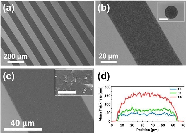
Piezoelectric inkjet printing offers a promising method for rapid prototyping and fabrication of printed electronic devices due to its non-contact, digital nature and broad materials compatibility. Inkjet printing of pristine graphene is an important capability for integrating graphene into printed devices, and has been reported using two general approaches: dispersing graphene directly in NMP with no binder 20,28 and using EC to stabilize graphene in a variety of solvents. 18,27 Key results using both of these methods are listed in Table 1. While binder-free dispersion of graphene reduces the requirement for thermal annealing, it offers less versatility to tailor the ink properties such as viscosity and surface tension. Using EC, the solvent system can be tuned to produce stable, high-concentration graphene inks that produce patterns with excellent morphology. Representative images of such patterns are shown in Figure 2, including lines following a single printing pass and dense graphene lines generated from multiple-pass printing. These lines exhibit no evidence of coffee ring formation, and have a reasonable resolution of approximately 60 µM. These patterns were generated using a Fujifilm Dimatix Materials Printer (DMP-2800) equipped with a 10 pL cartridge (DMC-11610) on a SiO 2/Si wafer treated with hexamethyldisilazane (HMDS). Importantly, similar patterns can be attained on untreated and O 2 plasma-treated SiO 2/Si wafers, glass slides, and Kapton TM films.
Table 1Inkjet printing of pristine graphene


Figure 2.Morphology of inkjet printed graphene features on HMDS-treated Si/SiO 2. Scanning electron micrographs of (a) multiple printed lines and (b) a single printed line and drop (inset, scale bar corresponds to 40 μm) illustrate the uniformity of the printed features. (c) SEM image of a graphene line printed with multiple passes and close-up image showing the resulting dense film microstructure (inset, scale bar = 1 µm). (d) Film cross-section as measured by AFM, averaged over approximately 20 µm of line length for 1, 3, and 10 printing passes.
GRAVURE PRINTABLE GRAPHENE INK
Gravure printing is ideally suited to high-throughput, roll-to-roll patterning for large-scale production of printed electronics. 29 Inks for gravure printing require a high solids loading and well-controlled viscosity and surface tension. Graphene inks have been developed for gravure printing based on EC and terpineol. 30 With a solids loading of 10% wt. and a viscosity of 0.75-3 Pa•s, this ink has been printed using a direct gravure printing system to produce patterns with a resolution of approximately 30 µM, as shown in Figure 3. The graphene patterns produced by this method exhibit a film morphology and conductivity that is similar to inkjet-printed patterns. The rheological properties of graphene inks developed for inkjet and gravure printing are listed in Table 2

Figure 3.Characterization of gravure printed graphene lines. (a) Line width and (b) line thickness for varying cell size, measured prior to annealing by optical microscopy and optical profilometry, respectively. (c) Large-area scanning electron micrograph of printed lines. (d) Line height profiles measured prior to annealing by optical profilometry, averaged over approximately 2 mm of line length.
Table 2Graphene inks for inkjet and gravure printing
GRAPHENE FILM CHARACTERISTICS
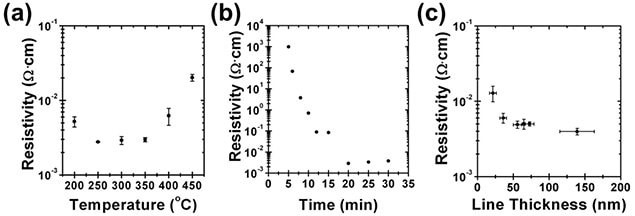
The properties of solution-processed graphene films depend on the microstructure of the graphene flake network. The two-dimensional structure of graphene is well-suited for producing dense films, but flake aggregation during solvent evaporation can prevent the formation of a uniform film. The inkjet and gravure inks highlighted previously mitigate this problem through the use of the EC binder. This binder effectively isolates the flakes as the ink dries, so the as-deposited films must be thermally annealed to exhibit optimal conductivity. As shown in Figure 4, an annealing treatment in air at 250 °C results in patterns with a high conductivity of approximately 25000 S/m, even for patterns as thin as 150 nM.
Figure 4.Electrical characteristics of graphene films. (a) Resistivity of graphene films with different annealing temperatures (30 minutes annealing). (b) Resistivity of graphene films annealed at 250 °C for various times. (c) Resistivity of inkjet-printed graphene lines plotted against line thickness.
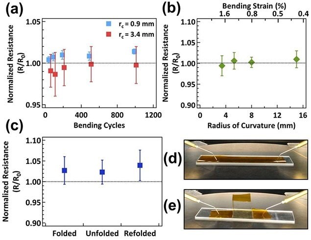
In addition to high electrical conductivity, the printed graphene films exhibit a robust tolerance to bending stresses. As shown in Figure 5, graphene lines printed on Kapton TM showed no measureable change in resistance while strained (tensile strain) to a radius of 4 mm. 27 In addition, the lines also retain their electrical properties when subjected to 1000 bending cycles at a radius of curvature of <1 mm. Finally, graphene lines exhibited only a small increase in resistance when folded.
Figure 5.Flexibility characteristics of printed graphene lines on Kapton™ substrates. (a) Resistance of graphene lines folded to a radius of curvature of 0.9 and 3.4 mm, normalized to the resistance prior to bending. (b) Normalized resistance of graphene lines measured in a flexed state for various degrees of bending, showing reliable retention of electrical conductivity across all measured flex states. (c) Normalized resistance of graphene lines while measured in a folded state, showing a small and irreversible increase in resistance following folding. Images of the sample in the (d) original and (e) folded state.
APPLICATIONS OF PRINTED GRAPHENE
Graphene has been employed for a variety of applications in printed and flexible electronics due to its unique structure and properties. With a conductivity of approximately 25000 S/m, the graphene films described here offer electrical properties comparable to conductive polymer blends while offering a unique set of stability and materials compatibility characteristics. This combination of properties is particularly relevant for thin-film applications, such as contact modification for organic TFTs (OTFTs) and corrosion-resistant conductive coatings. Several studies have demonstrated enhanced charge injection for OTFTs using reduced graphene oxide (RGO) electrodes due to the induced morphology of the semiconductor on the electrode surface. 19,31 In addition, graphene electrodes have been employed in carbon nanotube TFTs with promising results. 32 Graphene also offers unique characteristics, such as a high surface area, for electrochemical applications including chemical and biological sensors and supercapacitors. 21 A brief overview of demonstrated applications for solution-processed graphene is included in Table 3, while a more comprehensive review can be found elsewhere. 21
Table 3Applications of printed graphene
SUMMARY
We have shown that stable, high concentration graphene inks can be developed using a stabilizing polymer system. This material system enables broad tuning of the rheology and other fluid properties to realize inks for inkjet and gravure printing. In addition, flake aggregation is mitigated to yield dense and highly conductive graphene films following thermal annealing. The ability to pattern graphene films using solution-based printing techniques enables a number of applications from conductive and stable surface coatings to electrodes for electrochemical sensors, thin-film transistors, and other printed devices.
References
1.Wood V, Panzer MJ, Chen J, Bradley MS, Halpert JE, Bawendi MG, Bulovic? V. 2009. Inkjet-Printed Quantum Dot-Polymer Composites for Full-Color AC-Driven Displays. Adv. Mater.. 21(21):2151-2155. http://dx.doi.org/10.1002/adma.200803256
2.Subramanian V, Frechet J, Chang P, Huang D, Lee J, Molesa S, Murphy A, Redinger D, Volkman S. 2005. Progress Toward Development of All-Printed RFID Tags: Materials, Processes, and Devices. Proc. IEEE. 93(7):1330-1338. http://dx.doi.org/10.1109/jproc.2005.850305
3.Gaikwad AM, Whiting GL, Steingart DA, Arias AC. 2011. Highly Flexible, Printed Alkaline Batteries Based on Mesh-Embedded Electrodes. Adv. Mater.. 23(29):3251-3255. http://dx.doi.org/10.1002/adma.201100894
4.Hoth C, Choulis S, Schilinsky P, Brabec C. 2007. High Photovoltaic Performance of Inkjet Printed Polymer:Fullerene Blends. Adv. Mater.. 19(22):3973-3978. http://dx.doi.org/10.1002/adma.200700911
5.Jang J, Ha J, Cho J. 2007. Fabrication of Water-Dispersible Polyaniline-Poly(4-styrenesulfonate) Nanoparticles For Inkjet-Printed Chemical-Sensor Applications. Adv. Mater.. 19(13):1772-1775. http://dx.doi.org/10.1002/adma.200602127
6.Sokolov AN, Roberts ME, Bao Z. 2009. Fabrication of low-cost electronic biosensors. Materials Today. 12(9):12-20. http://dx.doi.org/10.1016/s1369-7021(09)70247-0
7.Ng TN, Schwartz DE, Lavery LL, Whiting GL, Russo B, Krusor B, Veres J, Bröms P, Herlogsson L, Alam N, et al. 2012. Scalable printed electronics: an organic decoder addressing ferroelectric non-volatile memory. Sci Rep. 2(1): http://dx.doi.org/10.1038/srep00585
8.Arias AC, MacKenzie JD, McCulloch I, Rivnay J, Salleo A. 2010. Materials and Applications for Large Area Electronics: Solution-Based Approaches. Chem. Rev.. 110(1):3-24. http://dx.doi.org/10.1021/cr900150b
9.Lupo D, Clemens W, Breitung S, Hecker K. 2013. OE-A Roadmap for Organic and Printed Electronics.1-26. http://dx.doi.org/10.1007/978-1-4614-3160-2_1
10.Cummins G, Desmulliez MP. 2012. Inkjet printing of conductive materials: a review. Circuit World. 38(4):193-213. http://dx.doi.org/10.1108/03056121211280413
11.Kamyshny A, Magdassi S. 2014. Conductive Nanomaterials for Printed Electronics. Small. 10(17):3515-3535. http://dx.doi.org/10.1002/smll.201303000
12.Fuller S, Wilhelm E, Jacobson J. 2002. Ink-jet printed nanoparticle microelectromechanical systems. J. Microelectromech. Syst.. 11(1):54-60. http://dx.doi.org/10.1109/84.982863
13.Walker SB, Lewis JA. 2012. Reactive Silver Inks for Patterning High-Conductivity Features at Mild Temperatures. J. Am. Chem. Soc.. 134(3):1419-1421. http://dx.doi.org/10.1021/ja209267c
14.Rouhi N, Jain D, Burke PJ. 2011. High-Performance Semiconducting Nanotube Inks: Progress and Prospects. ACS Nano. 5(11):8471-8487. http://dx.doi.org/10.1021/nn201828y
15.Weiss NO, Zhou H, Liao L, Liu Y, Jiang S, Huang Y, Duan X. 2012. Graphene: An Emerging Electronic Material. Adv. Mater.. 24(43):5782-5825. http://dx.doi.org/10.1002/adma.201201482
16.Dua V, Surwade S, Ammu S, Agnihotra S, Jain S, Roberts K, Park S, Ruoff R, Manohar S. 2010. All-Organic Vapor Sensor Using Inkjet-Printed Reduced Graphene Oxide. Angew. Chem. Int. Ed.. 49(12):2154-2157. http://dx.doi.org/10.1002/anie.200905089
17.Kong D, Le LT, Li Y, Zunino JL, Lee W. 2012. Temperature-Dependent Electrical Properties of Graphene Inkjet-Printed on Flexible Materials. Langmuir. 28(37):13467-13472. http://dx.doi.org/10.1021/la301775d
18.Li J, Ye F, Vaziri S, Muhammed M, Lemme MC, Östling M. 2013. Efficient Inkjet Printing of Graphene. Adv. Mater.. 25(29):3985-3992. http://dx.doi.org/10.1002/adma.201300361
19.Lim S, Kang B, Kwak D, Lee WH, Lim JA, Cho K. 2012. Inkjet-Printed Reduced Graphene Oxide/Poly(Vinyl Alcohol) Composite Electrodes for Flexible Transparent Organic Field-Effect Transistors. J. Phys. Chem. C. 116(13):7520-7525. http://dx.doi.org/10.1021/jp203441e
20.Torrisi F, Hasan T, Wu W, Sun Z, Lombardo A, Kulmala TS, Hsieh G, Jung S, Bonaccorso F, Paul PJ, et al. 2012. Inkjet-Printed Graphene Electronics. ACS Nano. 6(4):2992-3006. http://dx.doi.org/10.1021/nn2044609
21.Guo S, Dong S. 2011. Graphene nanosheet: synthesis, molecular engineering, thin film, hybrids, and energy and analytical applications. Chem. Soc. Rev.. 40(5):2644. http://dx.doi.org/10.1039/c0cs00079e
22.Mao S, Pu H, Chen J. 2012. Graphene oxide and its reduction: modeling and experimental progress. RSC Adv.. 2(7):2643. http://dx.doi.org/10.1039/c2ra00663d
23.Hernandez Y, Nicolosi V, Lotya M, Blighe FM, Sun Z, De S, McGovern IT, Holland B, Byrne M, Gun'Ko YK, et al. 2008. High-yield production of graphene by liquid-phase exfoliation of graphite. Nature Nanotech. 3(9):563-568. http://dx.doi.org/10.1038/nnano.2008.215
24.Paton KR, Varrla E, Backes C, Smith RJ, Khan U, O?Neill A, Boland C, Lotya M, Istrate OM, King P, et al. 2014. Scalable production of large quantities of defect-free few-layer graphene by shear exfoliation in liquids. Nature Mater. 13(6):624-630. http://dx.doi.org/10.1038/nmat3944
25.Liang YT, Hersam MC. 2010. Highly Concentrated Graphene Solutions via Polymer Enhanced Solvent Exfoliation and Iterative Solvent Exchange. J. Am. Chem. Soc.. 132(50):17661-17663. http://dx.doi.org/10.1021/ja107661g
26.Derby B. 2010. Inkjet Printing of Functional and Structural Materials: Fluid Property Requirements, Feature Stability, and Resolution. Annu. Rev. Mater. Res.. 40(1):395-414. http://dx.doi.org/10.1146/annurev-matsci-070909-104502
27.Secor EB, Prabhumirashi PL, Puntambekar K, Geier ML, Hersam MC. 2013. Inkjet Printing of High Conductivity, Flexible Graphene Patterns. J. Phys. Chem. Lett.. 4(8):1347-1351. http://dx.doi.org/10.1021/jz400644c
28.Finn DJ, Lotya M, Cunningham G, Smith RJ, McCloskey D, Donegan JF, Coleman JN. Inkjet deposition of liquid-exfoliated graphene and MoS2nanosheets for printed device applications. J. Mater. Chem. C. 2(5):925-932. http://dx.doi.org/10.1039/c3tc31993h
29.Søndergaard RR, Hösel M, Krebs FC. 2013. Roll-to-Roll fabrication of large area functional organic materials. J. Polym. Sci. B Polym. Phys.. 51(1):16-34. http://dx.doi.org/10.1002/polb.23192
30.Secor EB, Lim S, Zhang H, Frisbie CD, Francis LF, Hersam MC. 2014. Gravure Printing of Graphene for Large-area Flexible Electronics. Adv. Mater.. 26(26):4533-4538. http://dx.doi.org/10.1002/adma.201401052
31.Becerril HA, Stoltenberg RM, Tang ML, Roberts ME, Liu Z, Chen Y, Kim DH, Lee B, Lee S, Bao Z. 2010. Fabrication and Evaluation of Solution-Processed Reduced Graphene Oxide Electrodes for p- and n-Channel Bottom-Contact Organic Thin-Film Transistors. ACS Nano. 4(11):6343-6352. http://dx.doi.org/10.1021/nn101369j
32.Su Y, Du J, Sun D, Liu C, Cheng H. 2013. Reduced graphene oxide with a highly restored ?-conjugated structure for inkjet printing and its use in all-carbon transistors. Nano Res.. 6(11):842-852. http://dx.doi.org/10.1007/s12274-013-0362-2
33.Huang L, Huang Y, Liang J, Wan X, Chen Y. 2011. Graphene-based conducting inks for direct inkjet printing of flexible conductive patterns and their applications in electric circuits and chemical sensors. Nano Res.. 4(7):675-684. http://dx.doi.org/10.1007/s12274-011-0123-z
34.Huang L, Wang Z, Pu J, Shen L, Zhang J. 2013. Graphene pattern by gravure printing for wireless strain sensor. 2013 Seventh International Conference on Sensing Technology (ICST); 02 Dec 2013; Wellington, New Zealand: IEEE. p. 387.
35.Shin K, Hong J, Jang J. 2011. Flexible and transparent graphene films as acoustic actuator electrodes using inkjet printing. Chem. Commun.. 47(30):8527. http://dx.doi.org/10.1039/c1cc12913a
36.Shin K, Hong J, Jang J. 2011. Micropatterning of Graphene Sheets by Inkjet Printing and Its Wideband Dipole-Antenna Application. Adv. Mater.. 23(18):2113-2118. http://dx.doi.org/10.1002/adma.201100345


