My Cart
0
You have no items in your shopping cart.
Creating an account has many benefits:
Product Manager
Sandra Forbes
Introduction
Over the last ten years, digital printing technologies have transitioned from merely visualizing information to generating functional outputs. The concept of "printing beyond color" encapsulates this shift. Although these technologies are still predominantly used for visual purposes, their advancement in creating functional outputs, particularly in printed electronics, has spurred a surge of innovative ideas and manufacturing methods, fostering lean production. The fundamental principle of digital printing involves the precise placement of microscopic liquid (ink) droplets or solid (toner) particles, directly linked to the information at each pixel of the image or text. This allows for the economical deposition of costly materials, whether functional or not, onto specific areas of a substrate, enabling selective deposition.
This article delves into inkjet printing, a pivotal digital fabrication technique and a cornerstone of printed electronics. It covers the classification of inkjet printing technology, discusses various aspects related to materials (inks, substrates), and explores pre-processing and post-processing steps. Additionally, it provides examples of applications, showcasing the diverse potential of inkjet-printed electronics. Ongoing research and development in functional materials and advanced printing equipment continue to drive daily innovations.
Printing technology is one of the most significant inventions that accelerated human progress by enabling the reliable transmission, exchange, and preservation of knowledge. Although Gutenberg's invention of the movable type printing press has been around for over five centuries, it was in the last century, with the advent of photography and, more importantly, the integration of printing with computerized information technology, that printing technologies diversified and became widely utilized.
The primary conventional printing technologies include offset, gravure, screen, and flexographic printing. These methods typically require a printing master or plate for each type of information (text, graphics, pictures) to be reproduced, necessitating an elaborate and sometimes cumbersome prepress process. Once preprocessed, these technologies, except for flatbed screen printing, can be used for rapid, large-scale production.
Unlike conventional methods, digital printing does not require a pre-manufactured master plate and applies minimal impact force to the substrate. The core principle of digital printing is the precise placement of microscopic liquid droplets or solid particles, directly linked to the information at each binary unit of the image. This eliminates the need for complex, time-consuming, and costly master creation and setup processes associated with conventional printing. Although digital printing may have lower throughput compared to high-end conventional methods, its versatility and adaptability have made it accessible to a broader audience, integrating seamlessly into existing manufacturing lines and revolutionizing sectors like small office/home office printing.
Digital printing technologies can be broadly categorized into two groups: (1) direct-to-substrate, which includes methods like inkjet and thermal transfer printing that apply information directly onto the substrate, and (2) direct-to-plate, which includes electrophotography and magnetography, where information is first transferred to a plate before being applied to the substrate.
While the terms "printed electronics" and "organic electronics" are often used interchangeably, they refer to distinct yet overlapping technologies. Printed electronics involves using printing techniques, both conventional and digital, to create electronic structures, devices, and circuits, regardless of the functional materials or substrates used, provided the materials can be processed from a liquid phase. Organic electronics, on the other hand, focuses on using organic materials, such as conductive polymers, to fabricate electronic structures on rigid or flexible substrates. Flexible electronics emphasize the use of bendable substrates like plastic or paper. The progress in printed electronics has opened new avenues for the design, fabrication, packaging, and application of electronic devices and circuits.
The additive nature of printing processes, the variety of materials that can be formulated as inks, and the ability to cater to different production scales, from prototyping to large-scale manufacturing, are key factors enabling the use of printing in electronics fabrication. While various printing technologies have been employed in printed electronics, screen printing and inkjet printing are predominant. Inkjet printing, in particular, is considered a key enabling technology due to its non-contact, mask-less, and master-less nature, allowing for precise material deposition on desired locations.
Inkjet printing technology generates ink droplets with diameters ranging from 10 to 150 μm, corresponding to the nozzle diameter, with droplet volumes in the picoliter range. This technology is particularly suited for printed electronics for several reasons:
·It is a non-contact process that selectively deposits a wide range of materials onto various substrates in a drop-by-drop manner.
·It requires less shop floor space, lower initial investment, and shorter commissioning time compared to other printing technologies.
·It is adaptable to a wide range of production scales, from prototyping to large-scale industrial production.
·It minimizes ink consumption and material wastage.
·It offers flexibility in positioning within a process chain.
·It can produce patterned thin films, essential for organic electronics.
However, for highly complex integrated circuits (ICs), specialized techniques beyond standard inkjet printing are required to achieve the necessary spatial resolution for ultra-short transistor channel lengths.
The inkjet technology is broadly classified into two categories, based on the mechanism of droplet generation. They are continuous inkjet (CIJ) and drop-on-demand inkjet (DOD). DOD printing is, in turn, classified into three types, namely thermal inkjet, piezo inkjet and electrostatic inkjet.
Despite its high droplet generation frequencies ranging from 20 to 60 kHz, CIJ printing is not extensively employed in printed electronics due to the risk of ink contamination during the recycling process after environmental exposure. Additionally, CIJ can be inherently wasteful, as it continually produces droplets regardless of whether each pixel of the image or text to be replicated contains information. Nevertheless, CIJ exhibits an advantage when utilized on substrates with non-planar geometries.
As far as the DOD inkjet technologies are concerned, thermal inkjet and electrostatic inkjet lag far behind the piezo inkjet,9 mainly due to the following reasons:
· Thermal inkjet can lead to degradation of functional materials present in the ink due to the cyclic thermal loading. Piezo inkjet, on the other hand, is an isothermal process. Nontheless, thermal inkjet has successfully proven suitable for the manufacturing of light-emitting diodes based on inorganic quantum dots.
· The range of ink solvents that could be used in piezo inkjet is much broader than thermal and electrostatic inkjet.
· The investment and running costs needed for an electrostatic inkjet is much higher than piezo inkjet. Moreover, this technique is still under development, and is not as mature as either piezo or thermal inkjet in its evolution.
As its name suggests, a piezo inkjet system comprises a piezoelectric transducer (PZT) that operates through the application of a voltage pulse, a phenomenon known as the inverse piezoelectric effect. In commercial printing applications, the frequency of these voltage pulses typically falls between 1 kHz and 20 kHz. The piezo actuation triggers the generation and propagation of pressure (acoustic) waves within the ink channel, leading to the formation of droplets at acoustic frequencies.
Figure 1a illustrates the commonly used bipolar waveform, along with a brief description of the significance of each segment of the waveform. This is just an example - many different types of waveforms can usually be applied to an inkjet printhead to create droplets. The profile and magnitude of the applied waveform depend on the nozzle dimensions, the rheology of the ink used, and the droplet size and velocity desired. Figure 1b shows a sequence of pictures depicting the formation of a droplet from a piezo inkjet nozzle.

Figure 1. a) Exemplary bipolar waveform for piezo actuation; b) Droplet formation sequence from the nozzle of a piezo inkjet printhead.
Requirements of Inkjet Printing
While the various inkjet printing technologies mentioned earlier share more or less similar requirements regarding materials, pre-processing of substrates, and post-processing of printed structures, this section specifically emphasizes the requirements for piezo inkjet printing.
Substrate: As noted earlier, inkjet printing is substrate-agnostic, allowing for the use of any type of substrate, whether rigid, flexible, reinforced, or non-reinforced. However, the interplay between the printed ink and the substrate is crucial in determining the precision and durability of the printed structure. Therefore, it is essential to achieve a good match between ink properties and substrate properties. Consequently, the substrate surface is commonly pre-treated before printing to enhance wetting, adhesion, and other factors. Plasma treatment and corona treatment are popular methods for this purpose. For achieving high-definition structures, substrate patterning—dividing the substrate surface into hydrophilic and hydrophobic areas—is utilized.
Inks: The inks utilized in printed electronics are dispersed (pigment-like) or dissolved (dye-like) in one or more solvents. These solvents serve as carriers, transporting functional materials through the printhead and ejecting them via the nozzle. In the realm of printed electronics, functional materials impart electronic/electrical properties such as conductivity, semiconductivity, resistivity, and dielectricity. Various types of inks fulfilling these functionalities are readily available in the market.
Key characteristics of piezo inkjet inks include a dynamic viscosity of less than 20 mPa·s, a surface tension value below 80 mN/m, stability of the ink in solution/suspension within the printhead, and a particle size of the ink constituents preferably much smaller than the nozzle orifice. These values serve as general guidelines and may vary depending on the specific system. Additionally, particle loading is a crucial factor determining the stability of the printing process.
Sintering/Curing: Unlike graphical printing, where functionality (light absorption and color) is achieved shortly after deposition and drying, functional inks used "beyond color" require a transformation of the deposited ink layer to impart functionality. This process removes solvents and other additives present in the ink, such as surfactants, dispersants, humectants, and adhesion enhancers. For instance, (pigment-like) metal nanoparticle inks require sintering to enable the nanoparticles to coalesce into a continuous, percolating structure that allows conductivity. Conversely, (dye-like) metal-organic decomposition (MOD) inks necessitate the breakdown of molecular complexes to form metal clusters. In both cases, sintering is typically achieved through the application of heat. For flexible plastic substrates that are thermally unstable, alternative sintering techniques such as continuous flash UV radiation, plasma treatment, laser-assisted sintering, microwave-assisted sintering, DC or AC electric fields, or chemical sintering have been proposed. Figure 2 illustrates the sintering sequence of a metal nanoparticle ink through the application of heat.
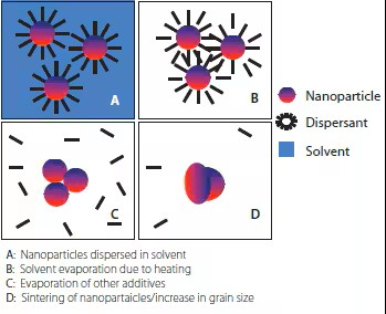
Figure 2. Sintering sequence of a metal nanoparticle based ink.
The quality of sintering is a critical concern. Despite sintering, the printed structures often fail to achieve 100% density due to the presence of residues. Furthermore, thermal sintering is not viable for all substrate types, as it typically requires temperatures exceeding 150 °C, which many polymer substrates cannot endure. In the case of organic polymer inks, the printed structure undergoes curing rather than sintering. Curing involves the hardening of polymers through cross-linking processes.
There are numerous application examples that demonstrate the suitability of inkjet printing for printed electronics; only a selected few are presented here.
Figure 3 shows one such application: an inkjet-printed planar dipole antenna for ultra-high frequency (UHF) range, on flexible and rigid substrates. Filter, transmission line, and patch antenna for the same frequency range have also been inkjet-printed and reported.
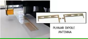
Figure 3. Inkjet printing of a planar dipole antenna with a resonance frequency of 868 MHz, using silver ink, at TU Chemnitz/Fraunhofer ENAS, Germany.
Inkjet printing has proven successful in the fabrication of passive electrical components and has even surpassed spin coating as a manufacturing method for organic or polymer light-emitting devices (OLED/PLED). Notably, high-resolution patterning of all-polymer thin-film transistors (TFTs) has been accomplished through inkjet printing. However, these devices are currently limited to low-end applications such as radio frequency identification tags (RFID) due to the low mobility of their active materials and slow switching speeds. Additionally, research in solar energy is an active field, with Konarka Technologies Inc. demonstrating inkjet-printed organic solar cells. Efforts are ongoing to inkjet print high-efficiency solar cells utilizing inorganic materials.
Inkjet printing holds immense potential to transform the manufacturing landscape of electronics. Despite the scarcity of fully inkjet-printed products in the market, significant efforts are being made to overcome existing challenges.
A pivotal factor in the success of inkjet printing for electronics applications lies in advancements in material development, particularly ink formulation. Inks containing high-performance functional materials that offer high mobility at lower sintering temperatures, combined with reliable printability, will facilitate the inkjet printing of high-performance electronic devices on diverse substrate materials. Moreover, the success of inkjet printing may hinge on the rapid maturation of alternative sintering and curing techniques, minimizing the heat exposure to printed flexible substrates. Lastly, the resolution of inkjet printing, which is inferior to photolithography, poses a limitation in its application for high-density circuit fabrication.
References
1. Kipphan H. 2001. Handbook of Print Media. https://doi.org/10.1007/978-3-540-29900-4
2. Océ Digital Printing. Océ Printing Systems GmbH, Germany(10th ed., 2006):
3. Printed Electronics: A Manufacturing Technology Analysis and Capability Forecast. NanoMarkets report: 2007 https://www.nanomarkets.net/
4. Parashkov R, Becker E, Riedl T, Johannes H, Kowalsky W. 2005. Large Area Electronics Using Printing Methods. Proc. IEEE. 93(7):1321-1329. https://doi.org/10.1109/jproc.2005.850304
5. de la Fuente Vornbrock A, Sung D, Kang H, Kitsomboonloha R, Subramanian V. 2010. Fully gravure and ink-jet printed high speed pBTTT organic thin film transistors. Organic Electronics. 11(12):2037-2044. https://doi.org/10.1016/j.orgel.2010.09.003
6. Derby B. 2010. Inkjet Printing of Functional and Structural Materials: Fluid Property Requirements, Feature Stability, and Resolution. Annu. Rev. Mater. Res.. 40(1):395-414. https://doi.org/10.1146/annurev-matsci-070909-104502
7. Sekitani T, Noguchi Y, Zschieschang U, Klauk H. 2008. Organic transistors manufactured using inkjet technology with subfemtoliter accuracy. PNAS. 105(13):4976-4980. https://doi.org/10.1073/pnas.0708340105
8. Wood V, Panzer MJ, Chen J, Bradley MS, Halpert JE, Bawendi MG, Bulovic V. 2009. Inkjet-Printed Quantum Dot-Polymer Composites for Full-Color AC-Driven Displays. Adv. Mater.. 21(21):2151-2155. https://doi.org/10.1002/adma.200803256
9. Sridhar A. An Inkjet Printing-Based Process Chain for Conductive Structures on Printed Circuit Board Materials. Ph.D. Thesis, University of Twente, the Netherlands, 2010
10. Herlogsson L, Noh YY, Zhao N, Crispin X, Sirringhaus H, Berggren M. 2008. Downscaling of Organic Field Effect Transistors with a Polyelectrolyte Gate Insulator. Adv. Mater.. 20(24):4708-4713. https://doi.org/10.1002/adma.200801756
11. Lim J, Lee W, Kwak D, Cho K. 2009. Evaporation-Induced Self-Organization of Inkjet-Printed Organic Semiconductors on Surface-Modified Dielectrics for High-Performance Organic Transistors. Langmuir. 25(9):5404-5410. https://doi.org/10.1021/la804269q
12. Wallace D, Shah V, Hayes D, Grove M. 1996. Imaging Sci. Technol. 40 5
13. Kamyshny A, Ben-Moshe M, Aviezer S, Magdassi S. 2005. Ink-Jet Printing of Metallic Nanoparticles and Microemulsions. Macromol. Rapid Commun.. 26(4):281-288. https://doi.org/10.1002/marc.200400522
14. de Gans B, Duineveld P, Schubert U. 2004. Inkjet Printing of Polymers: State of the Art and Future Developments. Adv. Mater.. 16(3):203-213. https://doi.org/10.1002/adma.200300385
15. de Gans B, Kazancioglu E, Meyer W, Schubert US. 2004. Ink-jet Printing Polymers and Polymer Libraries Using Micropipettes. Macromol. Rapid Commun.. 25(1):292-296. https://doi.org/10.1002/marc.200300148
16. Shin D, Smith PJ. 2008. Theoretical investigation of the influence of nozzle diameter variation on the fabrication of thin film transistor liquid crystal display color filters. Journal of Applied Physics. 103(11):114905. https://doi.org/10.1063/1.2936885
17. Jahn SF, Blaudeck T, Baumann RR, Jakob A, Ecorchard P, Ruffer T, Lang H, Schmidt P. 2010. Inkjet Printing of Conductive Silver Patterns by Using the First Aqueous Particle-Free MOD Ink without Additional Stabilizing Ligands. Chem. Mater.. 22(10):3067-3071. https://doi.org/10.1021/cm9036428
18. Yung K, Gu X, Lee C, Choy H. 2010. Ink-jet printing and camera flash sintering of silver tracks on different substrates. Journal of Materials Processing Technology. 210(15):2268-2272. https://doi.org/10.1016/j.jmatprotec.2010.08.014
19. Perelaer J, de Gans B, Schubert U. 2006. Ink-jet Printing and Microwave Sintering of Conductive Silver Tracks. Adv. Mater.. 18(16):2101-2104. https://doi.org/10.1002/adma.200502422
20. Allen ML, Aronniemi M, Mattila T, Alastalo A, Ojanperä K, Suhonen M, Seppä H. 2008. Electrical sintering of nanoparticle structures. Nanotechnology. 19(17):175201. https://doi.org/10.1088/0957-4484/19/17/175201
21. Allen M, Leppäniemi J, Vilkman M, Alastalo A, Mattila T. 2010. Substrate-facilitated nanoparticle sintering and component interconnection procedure. Nanotechnology. 21(47):475204. https://doi.org/10.1088/0957-4484/21/47/475204
22. Valeton JJP, Hermans K, Bastiaansen CWM, Broer DJ, Perelaer J, Schubert US, Crawford GP, Smith PJ. Room temperature preparation of conductive silver features using spin-coating and inkjet printing. J. Mater. Chem.. 20(3):543-546. https://doi.org/10.1039/b917266a
23. Harima Silver Nanopaste (NPS-J) Datasheet; Harima Chemicals Inc., Japan.
24. Sridhar A, Blaudeck T, Baumann R. 2011. Inkjet printing as a key enabling technology for printed electronics. . Material Matters. 6(1). 12-1 https://www.researchgate.net/publication/236074091_Inkjet_Printing_as_a_Key_Enabling_Technology_for_Printed_Electronics
25. Mäntysalo M, Mansikkamäki P. 2009. An inkjet-deposited antenna for 2.4 GHz applications. AEU - International Journal of Electronics and Communications. 63(1):31-35. https://doi.org/10.1016/j.aeue.2007.10.004
26. Ben-Tzvi P, Rone W. 2010. Microdroplet generation in gaseous and liquid environments. Microsyst Technol. 16(3):333-356. https://doi.org/10.1007/s00542-009-0962-7
27. Singh M, Haverinen HM, Dhagat P, Jabbour GE. 2010. Inkjet Printing: Inkjet Printing-Process and Its Applications (Adv. Mater. 6/2010). Adv. Mater.. 22(6):NA-NA. https://doi.org/10.1002/adma.201090011
Aladdinsci: https://www.aladdinsci.com