My Cart
0
You have no items in your shopping cart.
Creating an account has many benefits:

Introduction
The continuous development of solar energy technology is of great significance to human energy utilization. It is currently the cleanest and most abundant resource in the world. Solar energy can be harnessed in many ways, such as photovoltaic conversion and solar heating. The energy of solar radiation is 3.8×10 20 MW (3.8×10 20 M/s), and the energy reaching the earth is 173×10 6 kw (equivalent to 1360 W/m2). Although solar energy is huge, its low utilization efficiency has always been a headache. Silicon solar cells have a theoretical maximum efficiency of 31-40% due to material properties, but in actual deployment projects, the maximum panel efficiency only reaches 15-30%.
Therefore, maximizing the conversion of solar energy into electricity is a challenge. Researchers in related fields have proposed various solutions in solar cell technology to efficiently utilize the total solar energy received from the sun. Some of them are as follows:
●Use of nanocrystals made from the elements lead (Product No.:L121996) and selenium (Product No.:S105193) as solar cell raw materials
●Reduce solar cell manufacturing costs
●Building the basic unit of a solar cell from small cylinders or nanorods
●The use of dye-modified titanium dioxide (Product No.:T164497) material to increase the light absorption efficiency of solar cells 1-3
In addition to the above four points, there is also a record of using semiconductor materials to manufacture solar inverters with the aim of achieving high efficiency and reliability. Silicon carbide Product No.: S104650) is a third-generation semiconductor material that currently has a place in high-power applications due to its superior material properties. compared to silicon. Silicon carbide devices play a vital role in the fabrication of solar inverters. In photovoltaic energy conversion systems, the cost, performance and operation of the inverter are the main concerns. Today's inverters require improvements in parameters such as high reliability, high efficiency, enhanced communication, lower cost, and flexibility to support specialized applications. Typical photovoltaic inverter application scenarios are as follows:
● 1-10 kW for living applications
● 100 W to 300 kW for commercial applications
● 10-500 kW (2 MW ~ 20 MW in the future) for utility systems
The current focus is on improving volumetric power density (W/m3) and specific power (W/kg), thereby minimizing the cost of photovoltaic inverters. The application of SiC power semiconductor devices in photovoltaic cells can help solve several important problems.The current focus is on improving volumetric power density (W/m3) and specific power (W/kg), thereby minimizing the cost of photovoltaic inverters. The application of SiC power semiconductor devices in photovoltaic cells can help solve several important problems.
SiC for inverters in photovoltaic cells
50 kW three-phase photovoltaic inverter system
Commercial PV installations are typically rated from 100 kW to 1 MW and are especially suitable for commercial systems. In order to meet the needs of high-power photovoltaic systems, some research institutions have developed a 50kW photovoltaic inverter system prototype, which is the first full- SiC inverter with a specific power of 1kW/kg in the industry [4].
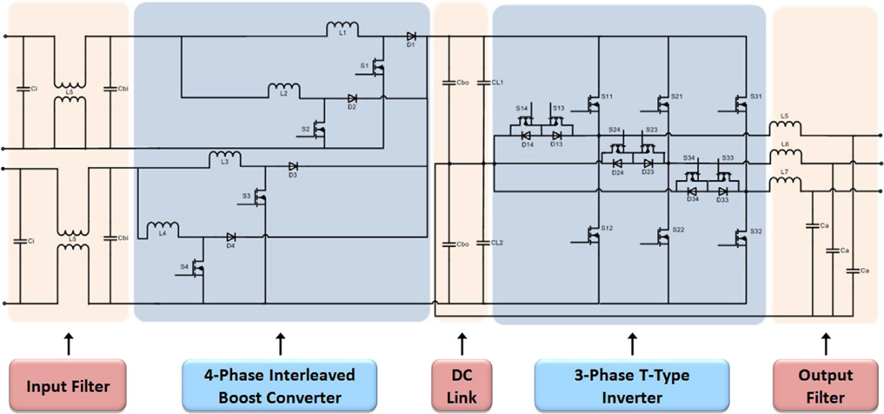
Figure 1: Simplified 50kw PV inverter circuit schematic showing various power conversion stages in the system
The power conversion process consists of 4 channels (12.5 kW per channel) interleaved boost converters and three phase inverters. The boost converter consists of two 20A SiC MOSFETs and two 1200 V/10 A SiC Schottky diodes in parallel. The boost converter operates at a switching frequency of 75 kHz and is more than 99% efficient at varying input voltages.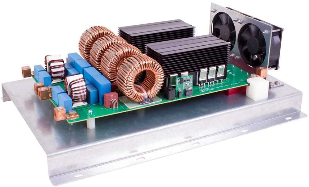
Figure 2: The hardware unit structure diagram of the photovoltaic inverter system of the 50kw boost converter part
5 kW three-phase inverter
In addition, some researchers have developed a 5 kW three-phase full- SiC inverter prototype using the XT-1000 half- bridge MOSFET module rated at 1200v/160a5. Figure 3 shows the final prototype and its internal structure, and although the inverter was not specifically designed for photovoltaic applications, it was able to demonstrate the ability of SiC power devices to increase their efficiency while reducing the size of the system. The switching frequency of this system is 50 kHz. The SiC inverter is compared with a commercial 5 kW silicon-based inverter 6 to quantify the performance parameters. Both systems use natural air convection for cooling. As can be seen from Figure 4, the SiC -based inverter can reduce losses by 27% compared to the silicon -based inverter.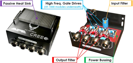
Figure 3: 5kW SiC three - phase inverter prototype and its internal structure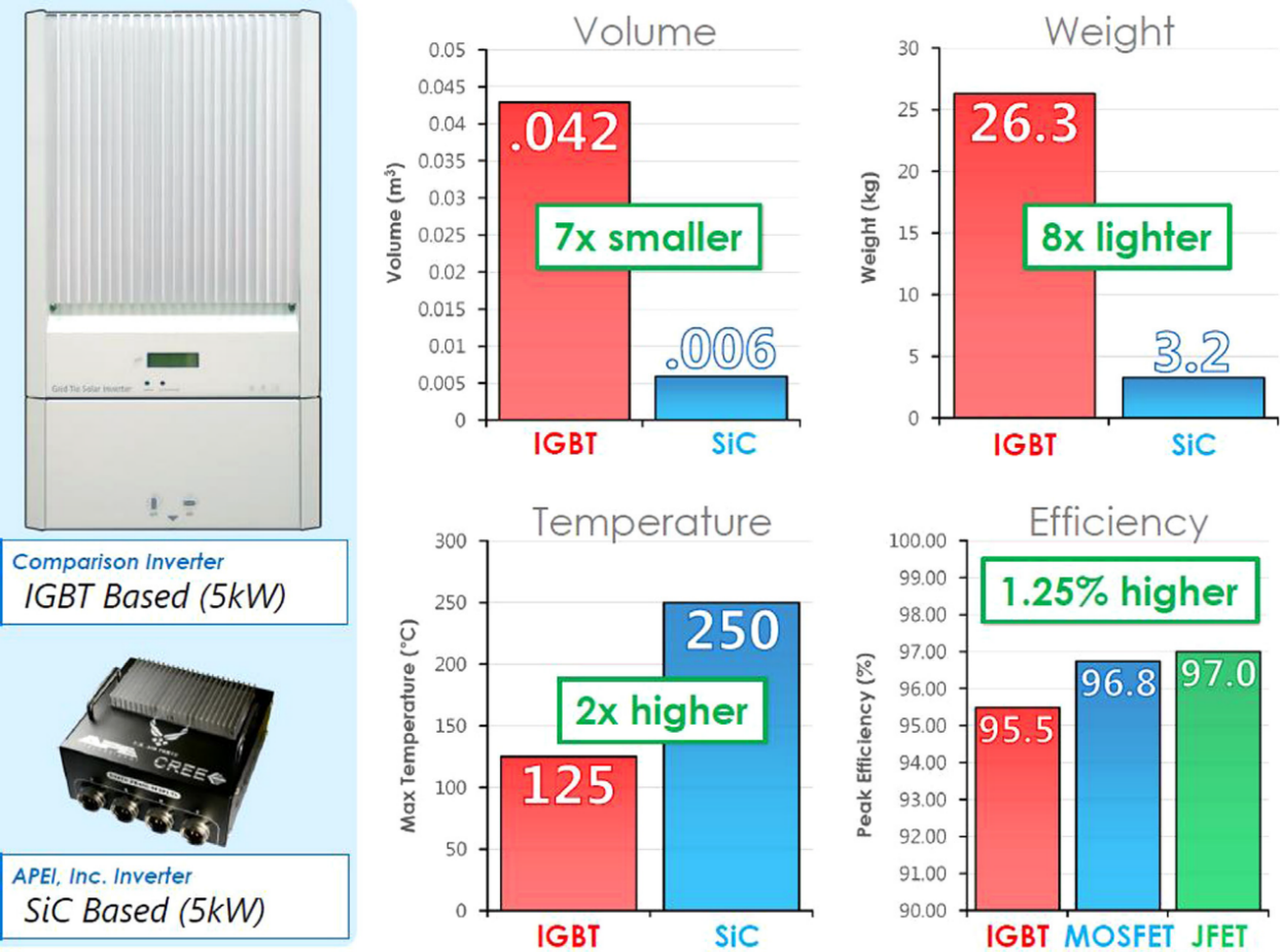
Figure 4: Advantages of SiC inverters over commercial silicon inverters (based on key performance parameters)
SiC for converters in photovoltaic cells
Amorphous non-stoichiometric silicon carbide (a- SixC1-x) is an ideal candidate for optoelectronic applications because of its wide tunable energy bandgap and ease of synthesis at lower substrate temperatures. Typically, stoichiometric SiC has a low absorption coefficient in the visible light region and exhibits poor electrical properties even after doping. To overcome these shortcomings, many studies in recent years have focused on the preparation of non-stoichiometric Six Ci1-x with tunable band gaps7,8. Non-stoichiometric SixC1-x 9,10 was synthesized by plasma-enhanced chemical vapor deposition (PECVD) by varying growth parameters such as substrate temperature. The process is similar to the synthesis of non - stoichiometric SiOx and SiNx materials. The tunable energy bandgap of non-stoichiometric SixCi1-x is strongly related to its C/Si composition, which in turn affects the absorption spectrum. During hydrogen-diluted PECVD, hydrogen carriers can reduce the density of surface defect states. However, preparation under hydrogen dilution usually requires higher substrate temperature and RF plasma power.
Under hydrogen-free PECVD, the non-stoichiometric Si-rich SixC1-x can be synthesized at lower substrate temperature, significantly improving its absorption coefficient. Compared with crystalline Si thin films, non-stoichiometric Si-rich SixCx materials have smaller optical band gaps and higher absorption coefficients in the visible region (400–600 nm). Many studies have reported the practical application of a-Si and SixC1-x hybrid PVSCs. However, few reports highlight all SixC1-x based PVSCs. Gao et al. 11 applied SixC1-x-based n-i-p junction PVSCs as semitransparent solar cells in light transmission modulators, but reported conversion efficiencies <1%. As shown in Figure 5, Lee et al. reduced the thickness of the n-type SixC1-x film based on p-n junction PVSCs of SixC1-x from 150 nm to 25 nm, and this parameter tuning reduced the conversion efficiency from 5 × 10 -3 % increased to 4.7% 12 .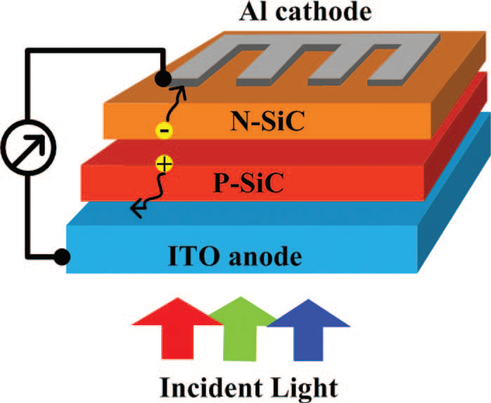
Figure 5: ITO/p- SiC /n- SiC /Al-based PVSC structures fabricated with n-type (thickness 25 ~ 100 nm) and p-type (thickness 50 nm) silicon-rich SiC films

Figure 6 : Band structure of Si x Ci 1-x /a-Si tandem PVSC
Conclusion
With the increasing global warming effect, carbon neutrality is imperative, which has injected great impetus into the development of the new energy field. The sun is the cleanest energy source, which makes the development and application of photovoltaic materials of great significance. Semiconductor materials with excellent properties such as silicon carbide are playing an important role in key devices such as photovoltaic converters and inverters, and will continue to contribute in the future.
References
[1] El Chaar L, El Zein N. Review of photovoltaic technologies[J]. Renewable and sustainable energy reviews, 2011, 15(5): 2165-2175. https://doi.org/10.1016/j.rser.2011.01.004
[2] Parida B, Iniyan S, Goic R. A review of solar photovoltaic technologies[J]. Renewable and sustainable energy reviews, 2011, 15(3): 1625-1636. https://doi.org/10.1016/j.rser.2010.11.032.
[3] Behar O, Khellaf A, Mohammedi K. A review of studies on central receiver solar thermal power plants[J]. Renewable and sustainable energy reviews, 2013, 23: 12-39. https://doi.org/10.1016/j.rser.2013.02.017.
[4] Mookken J, Agrawal B, Liu J. Efficient and compact 50kW Gen2 SiC device based PV string inverter[C]//PCIM Europe 2014; International Exhibition and Conference for Power Electronics, Intelligent Motion, Renewable Energy and Energy Management. VDE, 2014: 1-7. https://ieeexplore.ieee.org/abstract/document/6841306.
[5] Pushpakaran B N, Subburaj A S, Bayne S B, et al. Impact of silicon carbide semiconductor technology in Photovoltaic Energy System[J]. Renewable and Sustainable Energy Reviews, 2016, 55: 971-989. https://doi.org/10.1016/j.rser.2015.10.161.
[6] Bhalla A. Market Penetration of Wide-Bandgap SiC and GaN technology in light of Silicon Super junction and IGBT technology evolution[C]//CS MANTECH Conference. 2014: 9-12.
[7] Lin G R, Lo T C, Tsai L H, et al. Finite silicon atom diffusion induced size limitation on self-assembled silicon quantum dots in silicon-rich silicon carbide[J]. Journal of The Electrochemical Society, 2011, 159(2): K35.https://iopscience.iop.org/article/10.1149/2.014202jes/meta.
[8] Lo T C, Tsai L H, Cheng C H, et al. Self-aggregated Si quantum dots in amorphous Si-rich SiC[J]. Journal of non-crystalline solids, 2012, 358(17): 2126-2129. https://doi.org/10.1016/j.jnoncrysol.2012.01.013.
[9] Cheng Q, Tam E, Xu S, et al. Si quantum dots embedded in an amorphous SiC matrix: nanophase control by non-equilibrium plasma hydrogenation[J]. Nanoscale, 2010, 2(4): 594-600. https://pubs.rsc.org/en/content/articlehtml/2010/nr/b9nr00371a.
[10] Cheng Q, Xu S, Long J, et al. Homogeneous nanocrystalline cubic silicon carbide films prepared by inductively coupled plasma chemical vapor deposition[J]. Nanotechnology, 2007, 18(46): 465601. https://iopscience.iop.org/article/10.1088/0957-4484/18/46/465601/meta.
[11] Gao W, Lee S H, Bullock J, et al. First a-SiC: H photovoltaic-powered monolithic tandem electrochromic smart window device[J]. Solar Energy Materials and Solar Cells, 1999, 59(3): 243-254. https://doi.org/10.1016/S0927-0248(99)00025-2.
[12] Lee C T, Tsai L H, Lin Y H, et al. A chemical vapor deposited silicon rich silicon carbide PN junction based thin-film photovoltaic solar cell[J]. ECS Journal of Solid State Science and Technology, 2012, 1(6): Q144. https://iopscience.iop.org/article/10.1149/2.005301jss/meta.
[13] Cheng C H, Chang J H, Wu C I, et al. Semi-transparent silicon-rich silicon carbide photovoltaic solar cells[J]. RSC advances, 2015, 5(46): 36262-36269. https://pubs.rsc.org/en/content/articlehtml/2015/ra/c4ra16998k.